13μm-wavelength phase-locked VCSEL arrays incorporating patterned tunnel junction
9
1.3 μ m-wavelength phase-locked VCSEL arrays incorporating patterned tunnel junction Lukas Mutter, Vladimir Iakovlev, Andrei Caliman, Alexandru Mereuta, Alexei Sirbu, and Eli Kapon Ecole Polytechnique Federale de Lausanne (EPFL), Laboratory of Physics of Nanostructures, CH 1015 Lausanne, Switzerland [email protected] Abstract: We report the fabrication and the performance of phase-locked VCSEL arrays emitting near 1310 nm wavelength. The arrays were fabri- cated using double wafer fusion by patterning a tunnel junction layer, which serves to define the individual single mode array elements. Phase-locking in both one-dimensional and two-dimensional array configurations was confirmed by means of far field and spectral measurements as well as theo- retical modeling. CW output powers of more than 12 mW were achieved. © 2009 Optical Society of America OCIS codes: (140.3290) Laser arrays; (140.3325) Laser coupling; (140.7260) Vertical cavity surface emitting lasers References and links 1. A. Furukawa, S. Sasaki, M. Hoshi, A. Matsuzono, K. Moritoh, and T. Baba, “High-power single-mode vertical- cavity surface-emitting lasers with triangular holey structure,” Appl. Phys. Lett. 85, 5161-5163 (2004). 2. M. W. Wiemer, R. I. Aldaz, D. A. B. Miller, and J. S. Harris, “A Single Transverse-Mode Monolithically Inte- grated Long Vertical-Cavity Surface-Emitting Laser,” IEEE Photon. Technol. Lett. 17, 1366-1368 (2005). 3. A. Mircea, A. Caliman, V. Iakovlev, A. Mereuta, G. Suruceanu, C. A. Berseth, P. Royo, A. Syrbu, and E. Kapon, “Cavity Mode - Gain Peak Tradeoff for 1320 nm Wafer-Fused VCSELs with 3 mW Single-Mode Emission Power and 10 Gb/s Modulation Speed up to 70 ◦ C,” IEEE Photon. Technol. Lett. 19, 121-123 (2007). 4. I. Kardosh, F. Demaria, F. Rinaldi, S. Menzel, and R. Michalzik, “High-Power Single Transverse Mode Vertical- Cavity Surface-Emitting Lasers With Monolithically Integrated Curved Dielectric Mirrors,” IEEE Photon. Tech- nol. Lett. 20, 2084-2086 (2008). 5. M. Grabherr, M. Miller, R. J¨ ager, R. Michalzik, U. Martin, H. J. Unhold, and K. J. Ebeling, “High-Power VC- SEL’s: Single Devices and Densely Packed 2-D-Arrays,” IEEE J. Sel. Top. Quantum Electron. 5, 495-502 (1999). 6. R. Shau, M. Ortsiefer, J. Rosskopf, G. B¨ ohm, F. K¨ ohler, and M. C. Amann, “Vertical-cavity surface-emitting laser diodes at 1.55 μ m with large output power and high operation temperature,” Electron. Lett. 37, 1295-1296 (2001). 7. M. Achtenhagen, A. Hardy, and E. Kapon, “Mode discrimination in vertical-cavity surface-emitting lasers in- cluding Bragg reflectors and limiting apertures,” Opt. Eng. 44, 104202 1-6 (2005). 8. M.Orenstein, E. Kapon, N. G. Stoffel, J. P. Harbison, L. T. Florenz, and J. Wullert, “Two-dimensional phase- locked arrays of vertical-cavity semiconductor lasers by mirror reflectivity modulation,” Appl. Phys. Lett. 58, 804-806 (1991). 9. M. Orenstein, E. Kapon, J. P. Harbison, L. T. Florenz, and N. G. Stoffel, “Large two-dimensional arrays of phase-locked vertical cavity surface emitting lasers,” Appl. Phys. Lett. 60, 1535-1337 (1992). 10. H. J. Yoo, A. Scherer, J. P. Harbison, L. T. Florenz, E. G. Paek, B. P. Van der Gaag, J. R. Hayes, A. Von Lehmen, E. Kapon, and Y. S. Kwon, “Fabrication of a two-dimensional phased array of vertical-cavity surface-emitting lasers,” Appl. Phys. Lett. 56, 1198-1200 (1990). 11. J. J. Raftery, A. C. Lehman, A. J. Danner, P. O. Leisher, A. V. Giannopoulos, and K. D. Choquette, “In-phase evanescent coupling of two-dimensional arrays of defect cavities in photonic crystal vertical cavity surface emit- ting lasers,” Appl. Phys. Lett. 89, 081119 1-3 (2006). (C) 2009 OSA 11 May 2009 / Vol. 17, No. 10 / OPTICS EXPRESS 8558 #107739 - $15.00 USD Received 18 Feb 2009; revised 16 Apr 2009; accepted 28 Apr 2009; published 6 May 2009
Transcript of 13μm-wavelength phase-locked VCSEL arrays incorporating patterned tunnel junction

1.3µm-wavelength phase-locked VCSELarrays incorporating patterned tunnel
junction
Lukas Mutter, Vladimir Iakovlev, Andrei Caliman, AlexandruMereuta, Alexei Sirbu, and Eli Kapon
Ecole Polytechnique Federale de Lausanne (EPFL), Laboratory of Physics of Nanostructures,CH 1015 Lausanne, Switzerland
Abstract: We report the fabrication and the performance of phase-lockedVCSEL arrays emitting near 1310 nm wavelength. The arrays were fabri-cated using double wafer fusion by patterning a tunnel junction layer, whichserves to define the individual single mode array elements. Phase-lockingin both one-dimensional and two-dimensional array configurations wasconfirmed by means of far field and spectral measurements as well as theo-retical modeling. CW output powers of more than 12 mW were achieved.
© 2009 Optical Society of America
OCIS codes: (140.3290) Laser arrays; (140.3325) Laser coupling; (140.7260) Vertical cavitysurface emitting lasers
References and links1. A. Furukawa, S. Sasaki, M. Hoshi, A. Matsuzono, K. Moritoh, and T. Baba, “High-power single-mode vertical-
cavity surface-emitting lasers with triangular holey structure,” Appl. Phys. Lett.85, 5161-5163 (2004).2. M. W. Wiemer, R. I. Aldaz, D. A. B. Miller, and J. S. Harris, “ASingle Transverse-Mode Monolithically Inte-
grated Long Vertical-Cavity Surface-Emitting Laser,” IEEEPhoton. Technol. Lett.17, 1366-1368 (2005).3. A. Mircea, A. Caliman, V. Iakovlev, A. Mereuta, G. Suruceanu, C. A. Berseth, P. Royo, A. Syrbu, and E. Kapon,
“Cavity Mode - Gain Peak Tradeoff for 1320 nm Wafer-Fused VCSELs with 3 mW Single-Mode Emission Powerand 10 Gb/s Modulation Speed up to 70◦C,” IEEE Photon. Technol. Lett.19, 121-123 (2007).
4. I. Kardosh, F. Demaria, F. Rinaldi, S. Menzel, and R. Michalzik, “High-Power Single Transverse Mode Vertical-Cavity Surface-Emitting Lasers With Monolithically Integrated Curved Dielectric Mirrors,” IEEE Photon. Tech-nol. Lett.20, 2084-2086 (2008).
5. M. Grabherr, M. Miller, R. Jager, R. Michalzik, U. Martin, H. J. Unhold, and K. J. Ebeling, “High-Power VC-SEL’s: Single Devices and Densely Packed 2-D-Arrays,” IEEEJ. Sel. Top. Quantum Electron.5, 495-502 (1999).
6. R. Shau, M. Ortsiefer, J. Rosskopf, G. Bohm, F. Kohler, and M. C. Amann, “Vertical-cavity surface-emittinglaser diodes at 1.55µm with large output power and high operation temperature,” Electron. Lett.37, 1295-1296(2001).
7. M. Achtenhagen, A. Hardy, and E. Kapon, “Mode discrimination in vertical-cavity surface-emitting lasers in-cluding Bragg reflectors and limiting apertures,” Opt. Eng.44, 104202 1-6 (2005).
8. M.Orenstein, E. Kapon, N. G. Stoffel, J. P. Harbison, L. T.Florenz, and J. Wullert, “Two-dimensional phase-locked arrays of vertical-cavity semiconductor lasers by mirror reflectivity modulation,” Appl. Phys. Lett.58,804-806 (1991).
9. M. Orenstein, E. Kapon, J. P. Harbison, L. T. Florenz, and N. G. Stoffel, “Large two-dimensional arrays ofphase-locked vertical cavity surface emitting lasers,” Appl. Phys. Lett.60, 1535-1337 (1992).
10. H. J. Yoo, A. Scherer, J. P. Harbison, L. T. Florenz, E. G. Paek, B. P. Van der Gaag, J. R. Hayes, A. Von Lehmen,E. Kapon, and Y. S. Kwon, “Fabrication of a two-dimensional phased array of vertical-cavity surface-emittinglasers,” Appl. Phys. Lett.56, 1198-1200 (1990).
11. J. J. Raftery, A. C. Lehman, A. J. Danner, P. O. Leisher, A. V. Giannopoulos, and K. D. Choquette, “In-phaseevanescent coupling of two-dimensional arrays of defect cavities in photonic crystal vertical cavity surface emit-ting lasers,” Appl. Phys. Lett.89, 081119 1-3 (2006).
(C) 2009 OSA 11 May 2009 / Vol. 17, No. 10 / OPTICS EXPRESS 8558#107739 - $15.00 USD Received 18 Feb 2009; revised 16 Apr 2009; accepted 28 Apr 2009; published 6 May 2009

12. D. G. Deppe, J. P. van der Ziel, N. Chand, G. J. Zydzik, and S. N. G. Chu, “Phase-coupled two-dimensionalAlxGa1−xAs-GaAs vertical-cavity surface-emitting laser array,” Appl. Phys. Lett.56, 2089-2091 (1990).
13. A.C. Lehman and K. D. Choquette, “One- and Two- DimensionalCoherently Coupled Implant-Defined Vertical-Cavity Laser Arrays,” IEEE Photon. Technol. Lett.19, 1421-1423 (2007).
14. A. C. Lehman, D. F. Siriani, and K. D. Choquette, “Two-dimensional electronic beam-steering with implant-defined coherent VCSEL arrays,” Electron. Lett.43, 1202-1203 (2007).
15. L. D. A. Lundeberg and E. Kapon, “Mode switching and beam steering in photonic crystal heterostructuresimplemented with vertical-cavity surface-emitting lasers,”Appl. Phys. Lett.90, 241115 1-3 (2007).
16. A. Syrbu and E. Kapon, “Long-Wavelength VCSELs Power - efficient answer,” Nature Photonics,3, 27-29(2009).
17. A. Mereuta, A. Syrbu, V. Iakovlev, A. Rudra, A. Caliman, G.Suruceanu, C. A. Berseth, E. Deichsel, and E.Kapon, “1.5µm VCSEL structure optimized for high-power and high-temperatrue operation,” J. Crystal Growth272, 520-525 (2004).
18. M. Arzberger, M. Lohner, G. Bohm, and M. C. Amann, “Low-resistivity p-side contacts for InP-based devicesusing buried InGaAs tunnel junction,” Electron. Lett.36, 87-88 (2000).
19. J. W. Goodman,Introduction to Fourier Optics, (Roberts & Company, Engelwood, Colorado, Third Edition,2005).
1. Introduction
Vertical cavity surface emitting lasers (VCSELs) can deliver single mode optical power as largeas few mW [1–4], limited by the small aperture required for maintaining sufficient discrimina-tion against higher order transverse modes. Higher powers can be obtained by increasing theVCSEL aperture, e.g., by resorting to broad area VCSEL configurations [5, 6]. However, suchbroad area devices have poor spatial mode discrimination [5, 7] and often exhibit filamenta-tion due to material and structural nonuniformity [8]. One effective way to avoid filamentationand reach high spatial mode discrimination is the use of phase-locked arrays of single modelasers. Such phase-locked arrays of VCSELs have been demonstrated and studied using the(In)GaAs/AlGaAs semiconductor system emitting in the< 1µm spectral range. Various ap-proaches for defining the single-element VCSELs within the arrays have been implemented,including mirror patterning by reflectivity modulation [8,9] or selective etching [10, 11] anddefinition of current apertures [12,13]. These arrays have shown reduction of spontaneous fila-mentation and optical disorder effects [8,10–13] as well ashigh transverse mode discrimination,typically in favour of the out-of-phase supermode [8, 10, 12]. Application of separate contactsto such arrays can also yield interesting beam steering and switching mechanisms [14,15].
Similar phase-locked arrays emitting at longer wavelengths, particularly above 1.3µm wave-length, would also be of interest for free space communications, illumination and bio-medicalapplications, particularly those requiring eye-safe laser beams. Recently, important progresshas been achieved with long wavelength (LW) VCSELs emitting at the 1300-2000 nm wave-length range using several techniques, noteably employinghybrid Distributed Bragg Reflec-tors (DBRs) and buried tunnel junctions (TJ) [3, 16, 17]. Single mode output power of severalmW has been obtained with such VCSELs at temperatures as highas 80◦C. Coherent out-put powers could be increased by phase-locking several suchsingle mode VCSELs in one- ortwo-dimensional array configurations. In particular, the LW-VCSEL fabrication approach us-ing double wafer fusion, which yielded record single mode power of 5 mW at the 1300 nm [3]and of 4 mW at the 1500 nm [17] wavebands, is attractive for defining the array element bystructuring the fused interfaces prior to the wafer fusion steps.
In the present report, we demonstrate for the first time to ourknowledge phase-locking ofVCSEL arrays emitting in the long wavelength regime, namelyat 1300 nm. The arrays wererealized by patterning the tunnel junction prior to its overgrowth followed by double waferfusion of the DBRs. Thus, a controlled distribution of the optical gain across the VCSEL arraycan be achieved. Phase-locking in several array configurations is confirmed by far field andspectral characterizations of the devices. The measured coherent output cw powers are up to
(C) 2009 OSA 11 May 2009 / Vol. 17, No. 10 / OPTICS EXPRESS 8559#107739 - $15.00 USD Received 18 Feb 2009; revised 16 Apr 2009; accepted 28 Apr 2009; published 6 May 2009

12 mW, more than twice as high as compared to the one of corresponding single mode emitters.Furthermore, prospects for reaching higher powers are discussed.
2. Array patterning
The VCSEL array structures described here incorporate an In(Al)GaAs/InP active cavityand fused bottom and top AlGaAs/GaAs distributed Bragg reflectors (DBRs), all grown byorganometallic vapor phase epitaxy with both good thermal heat dissipation and high reflec-tivity [3]. Optical gain is provided by a stack of six strained InGaAs/InAlGaAs quantum wellswith parameters optimized for emission near 1320 nm wavelength. A buried tunnel junctionlocated at the active part is employed for hole injection [18]. A cross section through the finalVCSEL array structure after double wafer fusion bonding andcontact deposition is shown inFig. 1(a). For a more detailed description of the growth and processing steps see [3,17]. At thecontact areas of the p- and n-contact two current spreading layers are inserted, allowing for auniform current distribution prior to injection into the active region. The current is then locallyinjected through the patterned buried tunnel junctions, which provides a well defined gain dis-tribution as well as refractive index profile across the otherwise uniform VCSEL wafer. Thetunnel junction pattern thus defines the array configurationand the individual emitter size. Atop view of the patterned VCSEL arrays is shown schematically in Fig. 1(b). The single elementVCSEL apertures have a diameter ofd = 6µm. The lattice pitch of the realized linear (1x4 and1x8) and two dimensional (2D) (2x4) arrays wasΛ = 8µm. Common p- and n-contacts wereemployed for the entire array.
n-contact
p-contact
bottom DBR
QWs
tunnel junction
aperturetop DBR
Λ
d
n-contact
p-contact
(a) (b)
output beams
current spreading
layers
Fig. 1. (a) Cross section through the VCSEL array structure. The carriers are locally in-jected through the tunnel junction apertures. (b) Top view of a 2x4 VCSELarray. For thedevices discussed here,Λ = 8µm andd = 6µm.
(C) 2009 OSA 11 May 2009 / Vol. 17, No. 10 / OPTICS EXPRESS 8560#107739 - $15.00 USD Received 18 Feb 2009; revised 16 Apr 2009; accepted 28 Apr 2009; published 6 May 2009

3. Emission characteristics
3.1. Output power
The light-voltage-current characteristics (LIV) for the 1x4, 1x8 and 2x4 VCSEL arrays weremeasured and compared with those of a single VCSEL fabricated on the same wafer servingas reference, having the same layer structure and tunnel junction aperture size. The charac-teristics, obtained under continuous wave operation at 20◦C, are summarized in Fig. 2. Thesingle VCSEL showed maximum output power of about 3 mW, limited by thermal roll-over.Increasing the number of elements to four (a 1x4 array) yields a considerable increase in theemission power to over 9 mW. The total emission power dependsnonlinearly on the numberof array elements. This trend becomes even more pronounced for the 1x8 array, for which thetotal emission power was slightly higher than 12 mW. The two dimensional 2x4 array, althoughhaving the same number of elements as the linear 1x8 array, shows a lower performance withrespect to the total output power (output as high as∼11 mW).
0 10 20 30 40 500
1
2
3
4
Vo
lta
ge
[V
]
single element
0 20 400
3
6
9
12
0 10 20 30 40 500
1
2
3
4
1x4 array
0 20 400
3
6
9
12
Po
we
r [m
W]
0 10 20 30 40 500
1
2
3
4
Vo
lta
ge
[V
]
Current [mA]
1x8 array
0 20 400
3
6
9
12
0 10 20 30 40 500
1
2
3
4
Current [mA]
2x4 array
0 20 400
3
6
9
12
Po
we
r [m
W]
(a) (b)
(c) (d)
Fig. 2. Light-current-voltage characteristics of (a) single VCSEL, (b) 1x4 array, (c) 1x8array and (d) 2x4 array structure under continuous wave operation at 20◦C. All devicesemit near 1320 nm wavelength.
A better insight into the dependence of the array performance on the array configuration isgained by plotting the average power per pixel versus the average injection current per pixel, asdepicted in Fig. 3. The threshold current per element is the lowest for the two dimensional array,about 1 mA per VCSEL element. The two linear 1x4 and the 1x8 arrays have the next lowestthreshold per pixel,∼1.3 mA, which is still considerably smaller than the threshold current ofthe single VCSEL (∼2 mA). This behaviour can be explained by mainly two effects:Firstly,current spreading contributes to the pumping of neighbouring VCSEL elements, which meansthat the effective average current per element scales nonlinearly with the number of neighboringarray elements; secondly, the losses of the optical modes inthe array configuration are smallerdue to lower modal absorption in the unpumped areas of the active region. Hence, the threshold
(C) 2009 OSA 11 May 2009 / Vol. 17, No. 10 / OPTICS EXPRESS 8561#107739 - $15.00 USD Received 18 Feb 2009; revised 16 Apr 2009; accepted 28 Apr 2009; published 6 May 2009

0 1 2 3 4 5 6 7 80
0.5
1
1.5
2
2.5
Average Current per Pixel [mA]
Ave
rag
e P
ow
er
pe
r P
ixe
l [m
W]
1x4single
1x82x4
Fig. 3. Average optical output power per pixel as a function of the average pumping currentper array element for the devices of Fig. 2: single VCSEL (dotted curve), linear 1x4 array(dashed), 1x8 array (fine dashed), and 2x4 array (solid curve).
current per element decreases with increasing number of nearest neighbours. The geometry ofthe array configuration also affects the thermal dissipation of the device and hence the current atwhich thermal roll-over is reached. As each VCSEL element acts as a heat source, the thermaldissipation is most efficient for the single VCSEL structure. Among the array configurations,heat dissipation is most efficient for the linear arrays. Indeed, we observe that thermal roll-over of the light-current characteristic occurs the earliest in the 2x4 array, and the latest in thesingle VCSEL structure (see Fig. 3). This limits the achievable power per pixel in the 2D arrayconfiguration.
3.2. Phase-locking of array elements
VCSELs show high longitudinal mode selectivity due to the short cavity, but on the other handtransverse mode competition in these devices can drastically degrade their degree of coherence.This is particularly the case with VCSEL arrays, in which thetransverse modes (supermodes)can have small difference in oscillation wavelength and modal gain. To investigate the coher-ence and spatial mode content of the VCSEL arrays discussed here, we measured their emissionspectra, near field and far field intensity patterns at different diode currents at room tempera-ture. Furthermore, in order to check the degree of spatial coherence of the VCSEL arrays, wecomputed the far field patterns corresponding to the measured near field patterns. The far fieldelectric distribution(FF) is related to near field(NF) electric field by the Fraunhofer approxi-mation of the diffraction integral:
FF(θx,θy) =ejkzej k
2z(x2+y2)
jλz
∫ ∞
−∞
∫ ∞
−∞NF(η ,ν)e− j 2π
λ (sinθxη+sinθyν)dηdν (1)
wherez is the position of the far field plane,k is the wavenumber,λ is the emission wavelength,and (η ,ν) and (x,y) are the coordinates in the near field and far field planes, respectively. Thediffraction angles are defined as sinθx = x/z and sinθy = y/z. To examine the consistency ofthe measured far field intensity distribution with the expected lasing in the highest order super-mode, we assumed a phase shift ofπ between neighbouring pixels in the near field intensitydistribution.
The results of the measurements and simulation are displayed in Fig. 4 for the case of a1x4 array; the features of a single VCSEL operating well above threshold are also shown, forreference. Below lasing threshold (I = 2 mA) the amplified spontaneous emission distribution
(C) 2009 OSA 11 May 2009 / Vol. 17, No. 10 / OPTICS EXPRESS 8562#107739 - $15.00 USD Received 18 Feb 2009; revised 16 Apr 2009; accepted 28 Apr 2009; published 6 May 2009

20µm
2mA
20µm
5.5mA
20µm
10mA
20µm
14mA
-10o -5o 0o 5o 10o
10o
5o
0o
-5o
-10o
1316 1318 1320−80
−60
−40
−20
dB
1316 1318 1320−80
−60
−40
−20
dB
1316 1318 1320−80
−60
−40
−20
dB
1316 1318 1320−80
−60
−40
−20
Wavelength [nm]
dB
20µm
8mA
1316 1318 1320−80
−60
−40
−20
dB
-10o -5o 0o 5o 10o
10o
5o
0o
-5o
-10o
-10o -5o 0o 5o 10o
10o
5o
0o
-5o
-10o
-10o -5o 0o 5o 10o
10o
5o
0o
-5o
-10o
-10o -5o 0o 5o 10o
10o
5o
0o
-5o
-10o
Near Field Far Field Spectrum
-10o -5o 0o 5o 10o
10o
5o
0o
-5o
-10o
Simulated Far Field
Fig. 4. Near fields (left column), far fields (middle column), and emission spectra (rightcolumn) of a linear 1x4 array (Ith ≈ 5.5 mA), and of a single VCSEL (Ith ≈ 2 mA) withthe same tunnel junction aperture diameter (top row), measured at different diode currentsusing a variable attenuator in order to use the full sensitivity range of the camera. Thebottom row shows the calculated far field pattern obtained using the measured near fieldintensity distributions close to the lasing threshold, i.e., at 5.5 mA and assuming out-of-phase electric fields in neighbouring pixels.
(C) 2009 OSA 11 May 2009 / Vol. 17, No. 10 / OPTICS EXPRESS 8563#107739 - $15.00 USD Received 18 Feb 2009; revised 16 Apr 2009; accepted 28 Apr 2009; published 6 May 2009
20µm
6mA
20µm
11mA
20µm
22mA
1316 1318 1320−80
−60
−40
−20
dB
1316 1318 1320−80
−60
−40
−20
dB
1316 1318 1320−80
−60
−40
−20
Wavelength [nm]
dB
-10o -5o 0o 5o 10o
10o
5o
0o
-5o
-10o
-10o -5o 0o 5o 10o
10o
5o
0o
-5o
-10o
-10o -5o 0o 5o 10o
10o
5o
0o
-5o
-10o
Near Field Far Field Spectrum
-10o -5o 0o 5o 10o
10o
5o
0o
-5o
-10o
Simulated Far Field
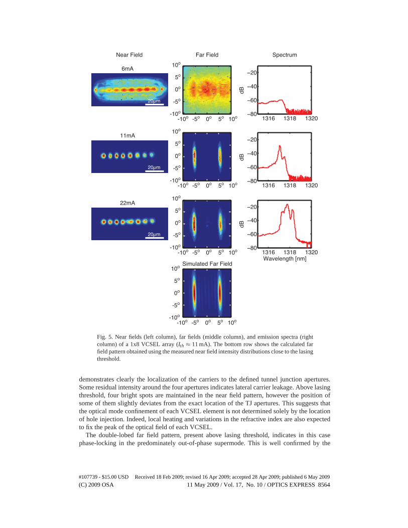
Fig. 5. Near fields (left column), far fields (middle column), and emission spectra (rightcolumn) of a 1x8 VCSEL array (Ith ≈ 11 mA). The bottom row shows the calculated farfield pattern obtained using the measured near field intensity distributions close to the lasingthreshold.
demonstrates clearly the localization of the carriers to the defined tunnel junction apertures.Some residual intensity around the four apertures indicates lateral carrier leakage. Above lasingthreshold, four bright spots are maintained in the near fieldpattern, however the position ofsome of them slightly deviates from the exact location of theTJ apertures. This suggests thatthe optical mode confinement of each VCSEL element is not determined solely by the locationof hole injection. Indeed, local heating and variations in the refractive index are also expectedto fix the peak of the optical field of each VCSEL.
The double-lobed far field pattern, present above lasing threshold, indicates in this casephase-locking in the predominately out-of-phase supermode. This is well confirmed by the
(C) 2009 OSA 11 May 2009 / Vol. 17, No. 10 / OPTICS EXPRESS 8564#107739 - $15.00 USD Received 18 Feb 2009; revised 16 Apr 2009; accepted 28 Apr 2009; published 6 May 2009

simulated far field distribution for which we used the measured near field intensity distributionclose to the lasing threshold, i.e., at 5.5 mA and assuming out-of-phase electric fields in neigh-bouring pixels. In particular, we note that at the corresponding current value the calculationsindicate virtually perfect coherence across the array, which is consistent with the fact that thecorresponding lasing spectra show predominantly a single lasing mode. Also, for higher drivingcurrents lasing in the out-of phase supermode is predominately present, which can be deducedfrom the evolution of the measured far field pattern.
20µm
4mA
8mA
20µm
16mA
1316 1318 1320−80
−60
−40
−20
dB
1316 1318 1320−80
−60
−40
−20
dB
1316 1318 1320−80
−60
−40
−20
Wavelength [nm]
dB
-10o -5o 0o 5o 10o
10o
5o
0o
-5o
-10o
-10o -5o 0o 5o 10o
10o
5o
0o
-5o
-10o
-10o -5o 0o 5o 10o
10o
5o
0o
-5o
-10o
20µm
Near Field Far Field Spectrum
Simulated Far Field
-10o -5o 0o 5o 10o
10o
5o
0o
-5o
-10o
Fig. 6. Near fields (left column), far fields (middle column), and spectra (right column) ofa 2x4 VCSEL array (Ith ≈ 8 mA). The bottom row shows the calculated far field patternobtained using the measured near field intensity distributions close to the lasingthreshold.
(C) 2009 OSA 11 May 2009 / Vol. 17, No. 10 / OPTICS EXPRESS 8565#107739 - $15.00 USD Received 18 Feb 2009; revised 16 Apr 2009; accepted 28 Apr 2009; published 6 May 2009

Whereas the emission spectrum of a single VCSEL made from the same wafer exhibits asingle transverse mode at∼ 1320nm wavelength with a high single mode suppression ration(SMSR), the spectra of the coupled array shows generally several modes. Near threshold, thearray lases at a single mode near∼ 1318 nm with SMSR> 20dB. At higher currents othermodes appear, representing other supermodes, which typically occur in multi-transverse modedevices.
Figure 5 shows the measured characteristics of a linear array consisting of 8 VCSEL ele-ments. The near field pattern below threshold reflects again the carrier distribution set by thepatterning of the tunnel junction. In addition to the 8 main spots corresponding to the tunneljunction apertures, one can notice two additional bright spots located at the extreme edges of thearray, which is probably due to light reflection from the edges of the etched mesa. Indeed, theseextra peaks do not evolve into lasing spots above threshold.The double-lobed far field patternindicates in this case as well phase-locking in predominantly the highest order supermode. Theemission spectrum shows a dominant mode near threshold, with additional modes joining inat higher currents. However, the spectral mode spacing is smaller than the corresponding spac-ings observed for either the single VCSEL or the 1x4 linear array, reflecting the larger globalaperture in the bigger array.
The emission characteristics of the 2x4 array are shown in Fig. 6. The evolution of the nearfield pattern shows that the highest intensity spots are again defined by the tunnel junction pat-terning below threshold, but above threshold an additionalrow of spots appears along the longerdimension of the array. This suggests that the tunnel junction patterning is relatively weak suchthat other mechanisms intervene in shaping the refractive index and/or gain distribution acrossthe global VCSEL array aperture. Nevertheless, this resultshows interesting engineering per-spectives; namely, that by altering the total size of the array aperture by means of changingthe distance between neighboring VCSELs different standing wave mode patterns could beexcited. The far field patterns above threshold show again the characteristic distribution of pre-dominantly the highest order supermode supported by a 2x5 array. The emission spectra exhibitas well the excitation of lower order supermodes, as expected with smaller spectral distancescompared to the previously considered structures, as expected.
4. Conclusion
We have realized 1D and 2D phase-locked arrays of VCSELs emitting at the 1300 nm wave-band. The structures were realized using double wafer fusion and tunnel junction patterning toproduce the desired definition of the individual VCSEL elements. Phase-locking of the struc-tures was confirmed by far field measurements and modeling, indicating operation at the out-of-phase supermode. Output power as high as 12 mW was achieved incontinuous wave at roomtemperature, limited by thermal dissipation. Higher powers might be achievable using largerarrays. However, special attention should be given to devising means for achieving efficientthermal dissipation and maintaining high uniformity in order to postpone multi mode opera-tion due to spatial hole burning. This approach of phase-locked VCSEL fabrication is flexi-ble, and should permit the realization of similar devices emitting between 1200 and 2000 nmwavelength. In particular, the possibility of separately patterning the tunnel junction and therefractive index across the array should prove useful for better control of the transverse modesin such devices.
(C) 2009 OSA 11 May 2009 / Vol. 17, No. 10 / OPTICS EXPRESS 8566#107739 - $15.00 USD Received 18 Feb 2009; revised 16 Apr 2009; accepted 28 Apr 2009; published 6 May 2009