1 Unit for Nanoscience and Technology, S.N.Bose …repository.ias.ac.in/42567/1/1-Auth.pdf · where...
9
arXiv:cond-mat/0607674v1 [cond-mat.mes-hall] 26 Jul 2006 Temperature dependence of the resistance of metallic nanowires (diameter ≥ 15 nm): Applicability of Bloch-Gr¨ uneisen theorem. Aveek Bid ∗1 , Achyut Bora 1 and A. K. Raychaudhuri †1,2 1 Department of Physics, Indian Institute of Science, Bangalore 560 012, India 2 Unit for Nanoscience and Technology, S.N.Bose National Centre for Basic Sciences, Salt Lake, Kolkata 700098, India We have measured the resistances (and resistivities) of Ag and Cu nanowires of diameters ranging from 15 nm to 200 nm in the temperature range 4.2 K-300 K with the specific aim to assess the applicability of the Bloch-Gr¨ uneisen formula for electron phonon resistivity in these nanowires. The wires were grown within polymeric templates by electrodeposition. We find that in all the samples the resistance reaches a residual value at T=4.2 K and the temperature dependence of resistance can be fitted to the Bloch-Gr¨ uneisen formula in the entire temperature range with a well defined transport Debye temperature (ΘR). The value of Debye temperature obtained from the fits lie within 8% of the bulk value for Ag wires of diameter 15 nm while for Cu nanowires of the same diameter the Debye temperature is significantly lesser than the bulk value. The electron-phonon coupling constants (measured by α el-ph or αR) in the nanowires were found to have the same value as that of the bulk. The resistivities of the wires were seen to increase as the wire diameter was decreased. This increase in the resistivity of the wires may be attributed to surface scattering of conduction electrons. The specularity p was estimated to be about 0.5. The observed results allow us to obtain the resistivities exactly from the resistance and gives us a method of obtaining the exact numbers of wires within the measured array (grown within the template). PACS numbers: I. INTRODUCTION Resistivity (ρ) of a metallic nanowire is a topic of con- siderable current interest. For nanowires with diameters approaching molecular dimensions the transport is likely to be quantum in nature [1]. However,there is a consid- erable size range (diameter > few nm) where the issues of quantum transport (like quantized conductance) are not important. Yet the study of the resistivity of such nanowire is of interest because this is likely to be the di- mension of metallic interconnects in electronic devices in the near future. In this size regime the concepts of Boltz- mann transport are at its limits of applicability. A proper understanding of the resistivity in this regime is needed because it allows one to get a quantitative estimate of the resistance of the wire from its dimension without actually measuring it. In the regime where the width of the wire is a few tens of nm or less, it has been established ade- quately that ρ is not determined by the material alone but by its size as well [2, 3, 4, 5, 6]. For wires of these dimensions, the mean free path is comparable to or even larger than the wire width (particularly for clean wires) and one would expect the size effect to be operative. In this range, ρ typically increases as the width of the wire is decreased. This is a serious issue in interconnects as an increase in the resistance of the wire increases the propagation delay time constant of the system and hence slows down the speed of the device. Recent investigations have focused on understanding the size effect in wires of * Electronic mail: [email protected] † Electronic mail: [email protected] width < 100 nm so that a predictive relation can be ob- tained [2, 3, 4, 5, 6]. The problem gets complicated due to the added contribution of grain boundary scattering. The size effect (arising mainly from the surface scatter- ing) and the internal grain boundary scattering (along with scattering form impurities or point defects) consti- tute the temperature independent part of the resistivity and this shows up as the residual resistivity at T ≤ 20K in most metallic solids. (If the wire is disordered the resistivity instead of showing a constant residual value at the low temperature can show an upturn often associ- ated with effects such as localization [7].) Understanding these effects for a nanowire will thus give us a control on the residual resistivity of the nanowire. However, under- standing the residual resistivity alone is not enough to get a complete understanding of the ρ in nanowires because at room temperatures, for a good metallic nanowire, a substantial part of the resistivity should arise from the temperature dependent part which in a non-magnetic metal arises from the electron-phonon interaction [8]. A good estimate and a quantitative way of predicting the resistivity contribution from the electron-phonon interac- tion is thus needed. In this paper the principal focus is on the specific issue of the contribution of electron-phonon scattering to the resistivity of metallic nanowires and we establish by experiments to what extent such established theory as the Bloch-Gr¨ uneisen theory [8] is applicable as the wire diameter goes down to as small as 15 nm. Temperature dependence of the resistivity of nanowires have been studied both theoretically as well as experi- mentally [9, 10, 11, 12, 13, 14]. Previous experimen- tal studies on nanowires of elemental metals and alloys have established that in wires with diameter (or width) ≥ 15 nm, the temperature dependence of resistance is
Transcript of 1 Unit for Nanoscience and Technology, S.N.Bose …repository.ias.ac.in/42567/1/1-Auth.pdf · where...
arX
iv:c
ond-
mat
/060
7674
v1 [
cond
-mat
.mes
-hal
l] 2
6 Ju
l 200
6
Temperature dependence of the resistance of metallic nanowires (diameter ≥ 15 nm):Applicability of Bloch-Gruneisen theorem.
Aveek Bid∗1, Achyut Bora1 and A. K. Raychaudhuri†1,2
1Department of Physics, Indian Institute of Science, Bangalore 560 012, India2Unit for Nanoscience and Technology, S.N.Bose National Centre for Basic Sciences, Salt Lake, Kolkata 700098, India
We have measured the resistances (and resistivities) of Ag and Cu nanowires of diameters rangingfrom 15 nm to 200 nm in the temperature range 4.2 K-300 K with the specific aim to assess theapplicability of the Bloch-Gruneisen formula for electron phonon resistivity in these nanowires. Thewires were grown within polymeric templates by electrodeposition. We find that in all the samplesthe resistance reaches a residual value at T=4.2 K and the temperature dependence of resistancecan be fitted to the Bloch-Gruneisen formula in the entire temperature range with a well definedtransport Debye temperature (ΘR). The value of Debye temperature obtained from the fits liewithin 8% of the bulk value for Ag wires of diameter 15 nm while for Cu nanowires of the samediameter the Debye temperature is significantly lesser than the bulk value. The electron-phononcoupling constants (measured by αel−ph or αR) in the nanowires were found to have the same valueas that of the bulk. The resistivities of the wires were seen to increase as the wire diameter wasdecreased. This increase in the resistivity of the wires may be attributed to surface scattering ofconduction electrons. The specularity p was estimated to be about 0.5. The observed results allowus to obtain the resistivities exactly from the resistance and gives us a method of obtaining theexact numbers of wires within the measured array (grown within the template).
PACS numbers:
I. INTRODUCTION
Resistivity (ρ) of a metallic nanowire is a topic of con-siderable current interest. For nanowires with diametersapproaching molecular dimensions the transport is likelyto be quantum in nature [1]. However,there is a consid-erable size range (diameter > few nm) where the issuesof quantum transport (like quantized conductance) arenot important. Yet the study of the resistivity of suchnanowire is of interest because this is likely to be the di-mension of metallic interconnects in electronic devices inthe near future. In this size regime the concepts of Boltz-mann transport are at its limits of applicability. A properunderstanding of the resistivity in this regime is neededbecause it allows one to get a quantitative estimate of theresistance of the wire from its dimension without actuallymeasuring it. In the regime where the width of the wireis a few tens of nm or less, it has been established ade-quately that ρ is not determined by the material alonebut by its size as well [2, 3, 4, 5, 6]. For wires of thesedimensions, the mean free path is comparable to or evenlarger than the wire width (particularly for clean wires)and one would expect the size effect to be operative. Inthis range, ρ typically increases as the width of the wireis decreased. This is a serious issue in interconnects asan increase in the resistance of the wire increases thepropagation delay time constant of the system and henceslows down the speed of the device. Recent investigationshave focused on understanding the size effect in wires of
∗Electronic mail: [email protected]†Electronic mail: [email protected]
width < 100 nm so that a predictive relation can be ob-tained [2, 3, 4, 5, 6]. The problem gets complicated dueto the added contribution of grain boundary scattering.The size effect (arising mainly from the surface scatter-ing) and the internal grain boundary scattering (alongwith scattering form impurities or point defects) consti-tute the temperature independent part of the resistivityand this shows up as the residual resistivity at T ≤ 20Kin most metallic solids. (If the wire is disordered theresistivity instead of showing a constant residual valueat the low temperature can show an upturn often associ-ated with effects such as localization [7].) Understandingthese effects for a nanowire will thus give us a control onthe residual resistivity of the nanowire. However, under-standing the residual resistivity alone is not enough to geta complete understanding of the ρ in nanowires becauseat room temperatures, for a good metallic nanowire, asubstantial part of the resistivity should arise from thetemperature dependent part which in a non-magneticmetal arises from the electron-phonon interaction [8]. Agood estimate and a quantitative way of predicting theresistivity contribution from the electron-phonon interac-tion is thus needed. In this paper the principal focus is onthe specific issue of the contribution of electron-phononscattering to the resistivity of metallic nanowires and weestablish by experiments to what extent such establishedtheory as the Bloch-Gruneisen theory [8] is applicable asthe wire diameter goes down to as small as 15 nm.
Temperature dependence of the resistivity of nanowireshave been studied both theoretically as well as experi-mentally [9, 10, 11, 12, 13, 14]. Previous experimen-tal studies on nanowires of elemental metals and alloyshave established that in wires with diameter (or width)≥ 15 nm, the temperature dependence of resistance is
2
metallic reaching a residual resistivity at low tempera-ture (if the wires are not disordered [9]) with ρ ∝ T forT≥ 100 K. For wires with smaller diameter and width(typically ≤ 10 nm) the resistivity can have a negativetemperature coefficient. This has been seen in wires ofAu [9], AuPd alloy [10], Zn [11], Cu [12] and Sn [13](before it becomes superconducting at Tc ≈ 3.7 K).However, there has not been any experimental studythat specifically addresses this issue in well character-ized nanowires over an extensive range of temperaturesand wire diameters and analyzes the data quantitatively.With these objectives we have studied the resistance ofmetallic nanowires (silver and copper) as a function ofthe wire diameter (15 nm-200 nm) in the temperaturerange 4.2 K-300 K. The systematic investigation allows usto separate out the temperature independent part R(0)from the temperature dependent part δR(T ) (we writeR(T ) = R(0) + δR(T )). We analyzed the data in theframework of the Bloch-Gruneisen theory. This allowedus to estimate the effective Debye temperature from thetemperature dependence of the resistance. In addition, aclear evaluation of the residual resistivity allowed us toestablish the dependence of the resistivity on the diame-ter of the wire. To our knowledge this is the first experi-mental study of the resistance of metallic nanowires oversuch an extensive range of temperature and size wherethe applicability of the Bloch-Gruneisen formula has beentested quantitatively.
II. ELECTRONPHONON INTERACTION AND
THE BLOCH-GRUNEISEN FORMULA
The electron-phonon interaction and the Bloch-Gruneisen formula have been adequately discussed instandard text books [8]. However, for the purpose ofquick reference as well as for completeness we give theimportant relations briefly in this section. In a non-magnetic metallic crystalline solid the temperature de-pendence of the electrical resistivity arises mainly fromthe electron-phonon interaction [8] and can be explainedin the framework of the Boltzmann transport theory us-ing the Bloch-Gruneisen formula:
ρ(T ) = ρ(0) + ρel−ph(T )
ρel−ph(T ) = αel−ph(T
ΘR
)n
∫ ΘR
T
0
xn
(ex − 1)(1 − e−x)dx
(1)where ρ(0) is the residual resistivity due to defect scat-tering and is essentially temperature independent. Thetemperature dependent part of the resistivity ρel−ph(T )arises from electron-phonon interaction. The constant ngenerally takes the values 2,3 and 5 depending on thenature of interaction and for a non magnetic elementalmetal like Cu, Ag or Au with reasonable mean free pathn = 5. αel−ph is a constant that is ∝ λtrωD/ω2
p where λtr
is the electron-phonon coupling constant, ωD is the De-bye frequency and ωp is the plasma frequency [17]. ΘR isthe Debye temperature as obtained from resistivity mea-surements and matches very closely with the values ofDebye temperature obtained from specific heat measure-ments. In the case of bulk silver and copper with n=5ΘR ∼ 200 K and ∼ 320 K respectively [18].
In Bloch-Gruneisen formula, the phonons that con-tribute to the electron-phonon interaction are the acous-tic phonons and one can get a simple one parameter scal-ing of the temperature dependence of the resistivity (ρ)where the only relevant parameter is the Debye temper-ature ΘR. For the specific case of n = 5,
ρel−ph(T )
ρΘR
= αR(T
ΘR
)5∫ ΘR
T
0
x5
(ex − 1)(1 − e−x)dx (2)
where ρΘRis the resistivity at the temperature T = ΘR.
Thus the temperature dependence of the electrical resis-tance of a metal provides a useful method to estimateits effective Debye temperature. For acoustic phononsthe value of αR is 4.225 [19]. Even when there is anuncertainty in the physical dimensions (that introducesuncertainty in the determination of ρ from R) the aboverelation can be utilized because one can write
R(T ) − R4.2K
RΘR
=δR(T )
RΘR
=ρel−ph(T )
ρΘR
(3)
The measurements carried out in this paper also al-low us to investigate how the electron-phonon interac-tion gets modified in nanowires due to size-reduction andmanifests itself in the temperature dependence of the re-sistance. The lower limit of the integral in equation 1being zero is the result of a tacit assumption that weare dealing with bulk material and hence the system sizedoes not impose a boundary condition on the maximumallowed phonon wavelength. This assumption may nolonger be valid for wires of very small diameters. Thusthe lower limit in the integral will now have a finite non-zero value. We wanted to investigate at what diametersof the wire does the size really begin to affect the phononspectrum (and hence the electrical resistivity) of the wire.
III. EXPERIMENTAL
The nanowires of Ag and Cu with average diameters inthe range of 15 nm-200 nm and length 6µm were electro-chemically deposited using polycarbonate membranes astemplate from AgNO3 and CuSO4 respectively [20, 21].Schematic arrangement of the growth set-up is given infigure 1(a). During the growth, one of the electrodes wasattached to one side of the membrane while the otherelectrode was a micro-tip of radius of curvature ≃ 100µmfitted to a micropositioner. This electrode can be placedat a specific area on the membrane and the growth canthus be localized. The wires grow by filling the pores
3
from end to end and as soon as one or more wires com-plete the path from one electrode to the other the growthstops. The wires after growth can be removed from themembrane by dissolving the polymer in dichloromethane.This is needed for the microscopic characterization of thewires as described below. The wires after growth wereannealed at 375K for 24 hours in vacuum under a dc cur-rent of 1 mA. The post-deposition annealing is neededto stabilize the resistance of the wires. For all successivemeasurements the current through the sample was keptlower than 100 µA.
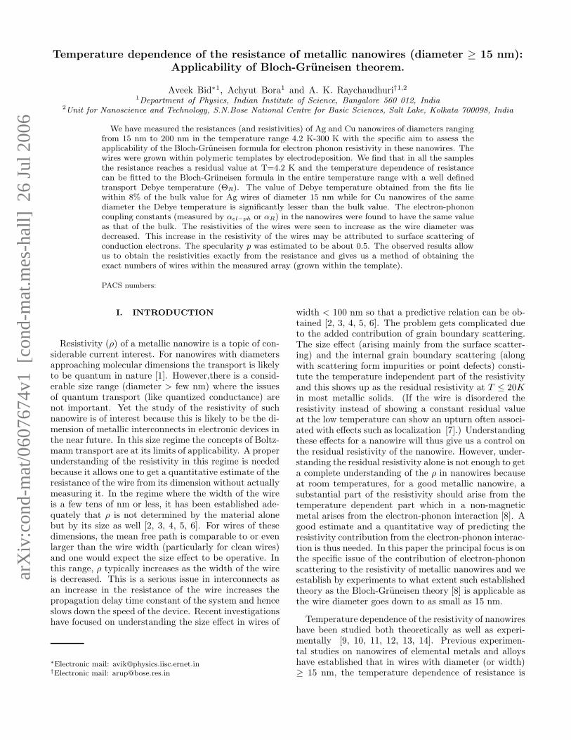
The structural and crystallographic nature of the wiresform an important part in the analysis of the data. Thewires used in this investigation are single crystalline innature. This has been established by such techniques asX-ray diffraction (XRD), Field Emission Gun-ScanningElectron Microscope (FEG-SEM) and High resolutiontransmission electron microscope (HRTEM). The TEMwas done in a Tecnai G2 30 machine operated at 300KVwith a nominal magnification of 106.
A
Cu base
micropositioner
membraneAgNO3
(a)
30 60 900
100
200
300
(222)
(311)(220)
(200)
(111)
Cou
nts (
a.u.
)
2q (radians)
FIG. 1: A schematic of the set up used for making thenanowires. (b) XRD of 100 nm Ag wires. The peaks havebeen indexed to FCC Ag.
IV. BASIC RESULTS
The XRD data are shown in figure 1(b). The XRDdata were indexed as FCC lattice. The data as shownin figure 1(b) does not show any impurity peak. Similardata were also obtained for Cu and are not shown toavoid duplicity.
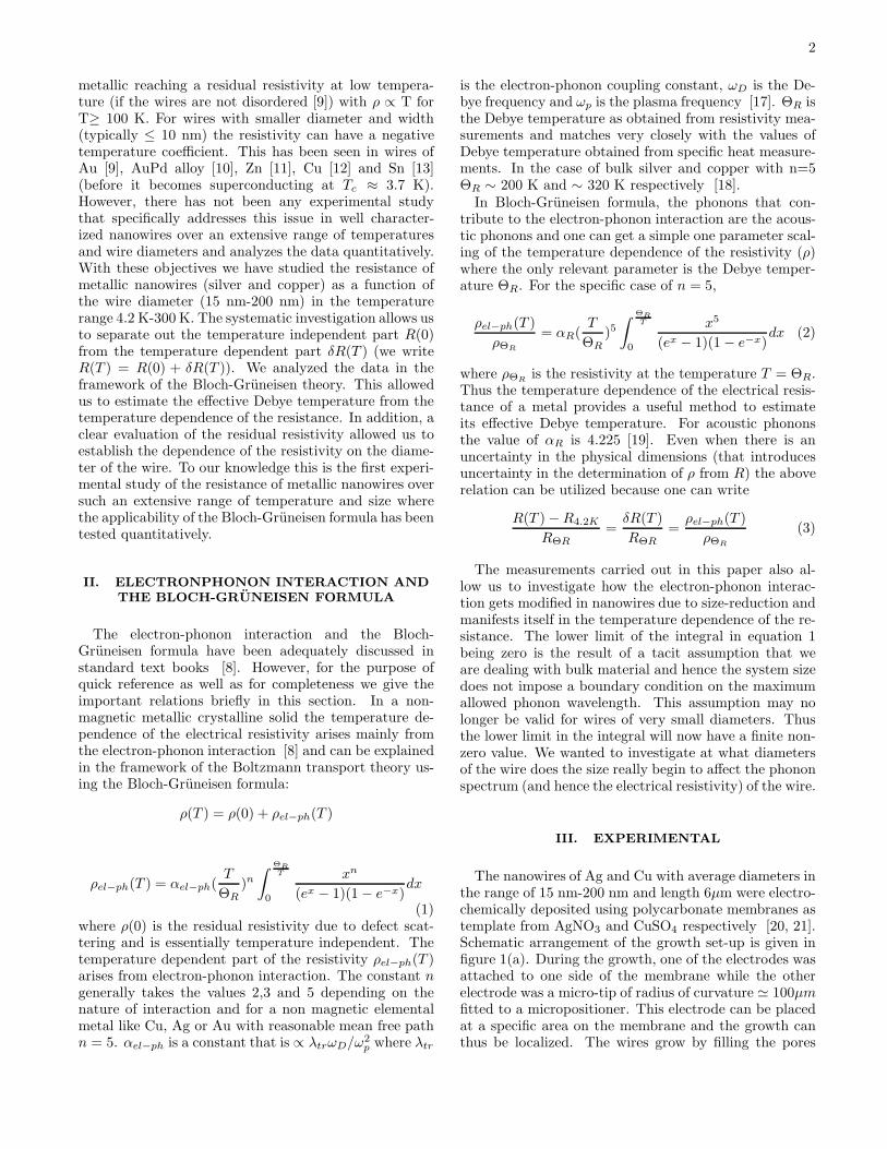
FIG. 2: SEM image of (a) 100 nm Ag wires taken after dis-solving off the template in dichloromethane, (b) SEM imageof a single 200 nm Ag wire.
Figure 2(a) shows the SEM image of a collection of Agnanowires of diameter 100 nm taken after partially re-moving the membrane while figure 2(b) shows the SEMimage of a single Ag wire of diameter 200 nm. The av-erage diameter of the wires match with the nominal di-ameter of the pores of the templates in which they weregrown.
In figure 3 we show a typical TEM data taken on a15 nm Ag wire. The diffraction data are also shown andcan be indexed into (220) planes. The TEM data showthat the wires are single crystalline with the presence oftwins in them. They also show that there are no othersubstantial structural defects like grain boundaries or dis-locations present in the sample. The growth direction asseen from the TEM data is [100].
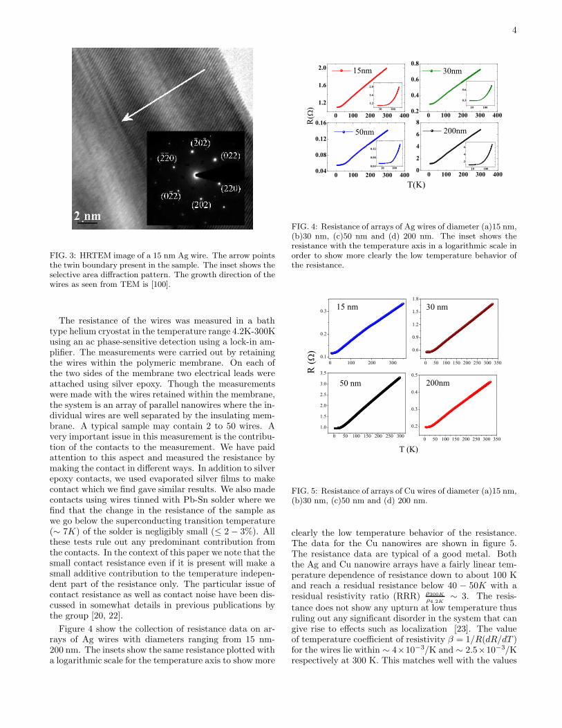
4
FIG. 3: HRTEM image of a 15 nm Ag wire. The arrow pointsthe twin boundary present in the sample. The inset shows theselective area diffraction pattern. The growth direction of thewires as seen from TEM is [100].
The resistance of the wires was measured in a bathtype helium cryostat in the temperature range 4.2K-300Kusing an ac phase-sensitive detection using a lock-in am-plifier. The measurements were carried out by retainingthe wires within the polymeric membrane. On each ofthe two sides of the membrane two electrical leads wereattached using silver epoxy. Though the measurementswere made with the wires retained within the membrane,the system is an array of parallel nanowires where the in-dividual wires are well separated by the insulating mem-brane. A typical sample may contain 2 to 50 wires. Avery important issue in this measurement is the contribu-tion of the contacts to the measurement. We have paidattention to this aspect and measured the resistance bymaking the contact in different ways. In addition to silverepoxy contacts, we used evaporated silver films to makecontact which we find gave similar results. We also madecontacts using wires tinned with Pb-Sn solder where wefind that the change in the resistance of the sample aswe go below the superconducting transition temperature(∼ 7K) of the solder is negligibly small (≤ 2 − 3%). Allthese tests rule out any predominant contribution fromthe contacts. In the context of this paper we note that thesmall contact resistance even if it is present will make asmall additive contribution to the temperature indepen-dent part of the resistance only. The particular issue ofcontact resistance as well as contact noise have been dis-cussed in somewhat details in previous publications bythe group [20, 22].
Figure 4 show the collection of resistance data on ar-rays of Ag wires with diameters ranging from 15 nm-200 nm. The insets show the same resistance plotted witha logarithmic scale for the temperature axis to show more
0 100 200 300 4000
2
4
6
80 100 200 300 400
1.2
1.6
2.0
0 100 200 300 4000.2
0.4
0.6
0.8
0 100 200 300 4000.04
0.08
0.12
0.16
10 100
1.2
1.6
2.0
10 100
0.3
0.6
10 1000.04
0.08
0.12
10 100
2
4
6
200nm
15nm
30nm
T(K)
50nm
R(W
)
FIG. 4: Resistance of arrays of Ag wires of diameter (a)15 nm,(b)30 nm, (c)50 nm and (d) 200 nm. The inset shows theresistance with the temperature axis in a logarithmic scale inorder to show more clearly the low temperature behavior ofthe resistance.
0 50 100 150 200 250 300 350
0.2
0.3
0.4
0.5
200nm
0 100 200 3000.1
0.2
0.3
15 nm
0 50 100 150 200 250 300 350
0.6
0.9
1.2
1.5
1.8
30 nm
0 50 100 150 200 250 300
1.0
1.5
2.0
2.5
3.0
3.5
T (K)
50 nm
R (W
)
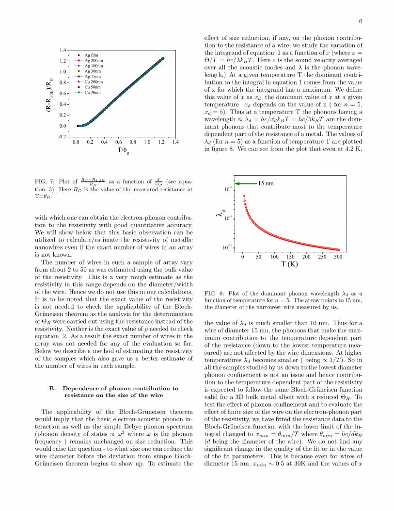
FIG. 5: Resistance of arrays of Cu wires of diameter (a)15 nm,(b)30 nm, (c)50 nm and (d) 200 nm.
clearly the low temperature behavior of the resistance.The data for the Cu nanowires are shown in figure 5.The resistance data are typical of a good metal. Boththe Ag and Cu nanowire arrays have a fairly linear tem-perature dependence of resistance down to about 100 Kand reach a residual resistance below 40 − 50K with aresidual resistivity ratio (RRR) ρ300K
ρ4.2K∼ 3. The resis-
tance does not show any upturn at low temperature thusruling out any significant disorder in the system that cangive rise to effects such as localization [23]. The valueof temperature coefficient of resistivity β = 1/R(dR/dT )for the wires lie within ∼ 4×10⁻³/K and ∼ 2.5×10⁻³/Krespectively at 300 K. This matches well with the values
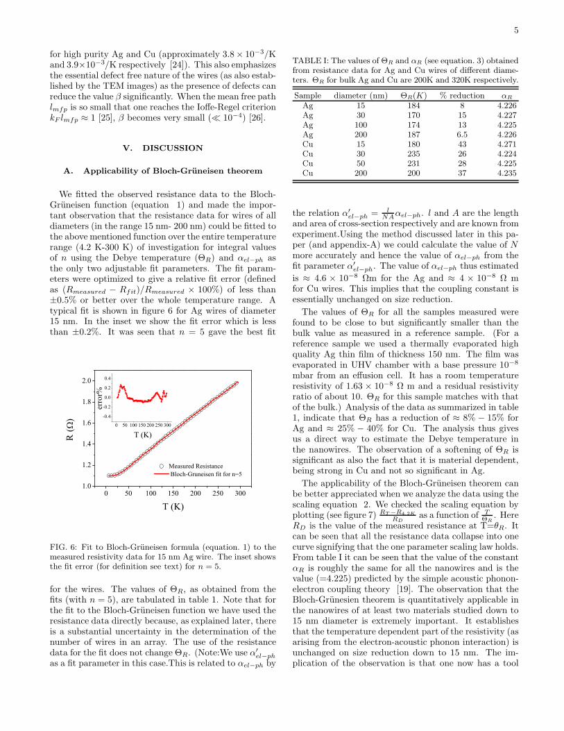
5
for high purity Ag and Cu (approximately 3.8× 10⁻³/Kand 3.9×10⁻³/K respectively [24]). This also emphasizesthe essential defect free nature of the wires (as also estab-lished by the TEM images) as the presence of defects canreduce the value β significantly. When the mean free pathlmfp is so small that one reaches the Ioffe-Regel criterionkF lmfp ≈ 1 [25], β becomes very small (≪ 10−4) [26].
V. DISCUSSION
A. Applicability of Bloch-Gruneisen theorem
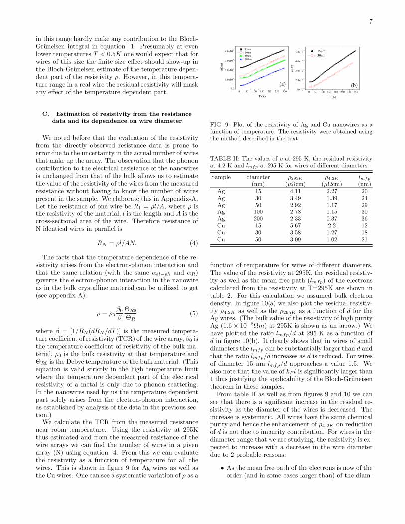
We fitted the observed resistance data to the Bloch-Gruneisen function (equation 1) and made the impor-tant observation that the resistance data for wires of alldiameters (in the range 15 nm- 200 nm) could be fitted tothe above mentioned function over the entire temperaturerange (4.2 K-300 K) of investigation for integral valuesof n using the Debye temperature (ΘR) and αel−ph asthe only two adjustable fit parameters. The fit param-eters were optimized to give a relative fit error (definedas (Rmeasured − Rfit)/Rmeasured × 100%) of less than±0.5% or better over the whole temperature range. Atypical fit is shown in figure 6 for Ag wires of diameter15 nm. In the inset we show the fit error which is lessthan ±0.2%. It was seen that n = 5 gave the best fit
0 50 100 150 200 250 3001.0
1.2
1.4
1.6
1.8
2.0
0 50 100 150 200 250 300
-0.4
-0.2
0.0
0.2
0.4
R (
)
T (K)
Measured Resistance Bloch-Gruneisen fit for n=5
err
or%
T (K)
FIG. 6: Fit to Bloch-Gruneisen formula (equation. 1) to themeasured resistivity data for 15 nm Ag wire. The inset showsthe fit error (for definition see text) for n = 5.
for the wires. The values of ΘR, as obtained from thefits (with n = 5), are tabulated in table 1. Note that forthe fit to the Bloch-Gruneisen function we have used theresistance data directly because, as explained later, thereis a substantial uncertainty in the determination of thenumber of wires in an array. The use of the resistancedata for the fit does not change ΘR. (Note:We use α′
el−ph
as a fit parameter in this case.This is related to αel−ph by
TABLE I: The values of ΘR and αR (see equation. 3) obtainedfrom resistance data for Ag and Cu wires of different diame-ters. ΘR for bulk Ag and Cu are 200K and 320K respectively.
Sample diameter (nm) ΘR(K) % reduction αR
Ag 15 184 8 4.226Ag 30 170 15 4.227Ag 100 174 13 4.225Ag 200 187 6.5 4.226Cu 15 180 43 4.271Cu 30 235 26 4.224Cu 50 231 28 4.225Cu 200 200 37 4.235
the relation α′el−ph = l
NAαel−ph. l and A are the length
and area of cross-section respectively and are known fromexperiment.Using the method discussed later in this pa-per (and appendix-A) we could calculate the value of Nmore accurately and hence the value of αel−ph from thefit parameter α′
el−ph. The value of αel−ph thus estimated
is ≈ 4.6 × 10⁻⁸ Ωm for the Ag and ≈ 4 × 10⁻⁸ Ω mfor Cu wires. This implies that the coupling constant isessentially unchanged on size reduction.
The values of ΘR for all the samples measured werefound to be close to but significantly smaller than thebulk value as measured in a reference sample. (For areference sample we used a thermally evaporated highquality Ag thin film of thickness 150 nm. The film wasevaporated in UHV chamber with a base pressure 10−8
mbar from an effusion cell. It has a room temperatureresistivity of 1.63 × 10⁻⁸ Ω m and a residual resistivityratio of about 10. ΘR for this sample matches with thatof the bulk.) Analysis of the data as summarized in table1, indicate that ΘR has a reduction of ≈ 8% − 15% forAg and ≈ 25% − 40% for Cu. The analysis thus givesus a direct way to estimate the Debye temperature inthe nanowires. The observation of a softening of ΘR issignificant as also the fact that it is material dependent,being strong in Cu and not so significant in Ag.
The applicability of the Bloch-Gruneisen theorem canbe better appreciated when we analyze the data using thescaling equation 2. We checked the scaling equation byplotting (see figure 7) RT −R4.2K
RD
as a function of TΘR
. HereRD is the value of the measured resistance at T=θR. Itcan be seen that all the resistance data collapse into onecurve signifying that the one parameter scaling law holds.From table I it can be seen that the value of the constantαR is roughly the same for all the nanowires and is thevalue (=4.225) predicted by the simple acoustic phonon-electron coupling theory [19]. The observation that theBloch-Grunesien theorem is quantitatively applicable inthe nanowires of at least two materials studied down to15 nm diameter is extremely important. It establishesthat the temperature dependent part of the resistivity (asarising from the electron-acoustic phonon interaction) isunchanged on size reduction down to 15 nm. The im-plication of the observation is that one now has a tool
6
0.0 0.2 0.4 0.6 0.8 1.0 1.2 1.4-0.2
0.0
0.2
0.4
0.6
0.8
1.0
1.2
1.4
(R
-R4.2K)/R
D
T/qR
Ag film Ag 200nm Ag 100nm Ag 30nm Ag 15nm Cu 200nm Cu 50nm Cu 30nm
FIG. 7: Plot of RT −R4.2K
RD
as a function of TΘR
(see equa-
tion. 3). Here RD is the value of the measured resistance atT=θR.
with which one can obtain the electron-phonon contribu-tion to the resistivity with good quantitative accuracy.We will show below that this basic observation can beutilized to calculate/estimate the resistivity of metallicnanowires even if the exact number of wires in an arrayis not known.
The number of wires in such a sample of array varyfrom about 2 to 50 as was estimated using the bulk valueof the resistivity. This is a very rough estimate as theresistivity in this range depends on the diameter/widthof the wire. Hence we do not use this in our calculations.It is to be noted that the exact value of the resistivityis not needed to check the applicability of the Bloch-Gruneisen theorem as the analysis for the determinationof ΘR were carried out using the resistance instead of theresistivity. Neither is the exact value of ρ needed to checkequation 2. As a result the exact number of wires in thearray was not needed for any of the evaluation so far.Below we describe a method of estimating the resistivityof the samples which also gave us a better estimate ofthe number of wires in each sample.
B. Dependence of phonon contribution to
resistance on the size of the wire
The applicability of the Bloch-Gruneisen theoremwould imply that the basic electron-acoustic phonon in-teraction as well as the simple Debye phonon spectrum(phonon density of states ∝ ω2 where ω is the phononfrequency ) remains unchanged on size reduction. Thiswould raise the question - to what size one can reduce thewire diameter before the deviation from simple Bloch-Gruneisen theorem begins to show up. To estimate the
effect of size reduction, if any, on the phonon contribu-tion to the resistance of a wire, we study the variation ofthe integrand of equation 1 as a function of x (where x =Θ/T = hc/λkBT . Here c is the sound velocity averagedover all the acoustic modes and λ is the phonon wave-length.) At a given temperature T the dominant contri-bution to the integral in equation 1 comes from the valueof x for which the integrand has a maximum. We definethis value of x as xd, the dominant value of x at a giventemperature. xd depends on the value of n ( for n = 5,xd = 5). Thus at a temperature T the phonons having awavelength ≈ λd = hc/xdkBT = hc/5kBT are the dom-inant phonons that contribute most to the temperaturedependent part of the resistance of a metal. The values ofλd (for n = 5) as a function of temperature T are plottedin figure 8. We can see from the plot that even at 4.2 K,
0 50 100 150 200 250 300
10-10
10-9
10-8
l d
T (K)
15 nm
FIG. 8: Plot of the dominant phonon wavelength λd as afunction of temperature for n = 5. The arrow points to 15 nm,the diameter of the narrowest wire measured by us.
the value of λd is much smaller than 10 nm. Thus for awire of diameter 15 nm, the phonons that make the max-imum contribution to the temperature dependent partof the resistance (down to the lowest temperature mea-sured) are not affected by the wire dimensions. At highertemperatures λd becomes smaller ( being ∝ 1/T ). So inall the samples studied by us down to the lowest diameterphonon confinement is not an issue and hence contribu-tion to the temperature dependent part of the resistivityis expected to follow the same Bloch-Gruneisen functionvalid for a 3D bulk metal albeit with a reduced ΘR. Totest the effect of phonon confinement and to evaluate theeffect of finite size of the wire on the electron-phonon partof the resistivity, we have fitted the resistance data to theBloch-Gruneisen function with the lower limit of the in-tegral changed to xmin = θmin/T where θmin = hc/dkB
(d being the diameter of the wire). We do not find anysignificant change in the quality of the fit or in the valueof the fit parameters. This is because even for wires ofdiameter 15 nm, xmin ∼ 0.5 at 30K and the values of x
7
in this range hardly make any contribution to the Bloch-Gruneisen integral in equation 1. Presumably at evenlower temperatures T < 0.5K one would expect that forwires of this size the finite size effect should show-up inthe Bloch-Gruneisen estimate of the temperature depen-dent part of the resistivity ρ. However, in this tempera-ture range in a real wire the residual resistivity will maskany effect of the temperature dependent part.
C. Estimation of resistivity from the resistance
data and its dependence on wire diameter
We noted before that the evaluation of the resistivityfrom the directly observed resistance data is prone toerror due to the uncertainty in the actual number of wiresthat make up the array. The observation that the phononcontribution to the electrical resistance of the nanowiresis unchanged from that of the bulk allows us to estimatethe value of the resistivity of the wires from the measuredresistance without having to know the number of wirespresent in the sample. We elaborate this in Appendix-A.Let the resistance of one wire be R1 = ρl/A, where ρ isthe resistivity of the material, l is the length and A is thecross-sectional area of the wire. Therefore resistance ofN identical wires in parallel is
RN = ρl/AN. (4)
The facts that the temperature dependence of the re-sistivity arises from the electron-phonon interaction andthat the same relation (with the same αel−ph and αR)governs the electron-phonon interaction in the nanowireas in the bulk crystalline material can be utilized to get(see appendix-A):
ρ = ρ0β0
β
ΘR0
ΘR
(5)
where β = [1/RN(dRN/dT )] is the measured tempera-ture coefficient of resistivity (TCR) of the wire array, β0 isthe temperature coefficient of resistivity of the bulk ma-terial, ρ0 is the bulk resistivity at that temperature andΘR0 is the Debye temperature of the bulk material. (Thisequation is valid strictly in the high temperature limitwhere the temperature dependent part of the electricalresistivity of a metal is only due to phonon scattering.In the nanowires used by us the temperature dependentpart solely arises from the electron-phonon interaction,as established by analysis of the data in the previous sec-tion.)
We calculate the TCR from the measured resistancenear room temperature. Using the resistivity at 295Kthus estimated and from the measured resistance of thewire arrays we can find the number of wires in a givenarray (N) using equation 4. From this we can evaluatethe resistivity as a function of temperature for all thewires. This is shown in figure 9 for Ag wires as well asthe Cu wires. One can see a systematic variation of ρ as a
0 50 100 150 200 250 3000.0
1.0x10⁻⁸
2.0x10⁻⁸
3.0x10⁻⁸
4.0x10⁻⁸
(a)
r(W
m)
T (K)
15nm 30nm 50nm 200nm
(b)0 50 100 150 200 250 300 350
1.0x10⁻⁸
2.0x10⁻⁸
3.0x10⁻⁸
4.0x10⁻⁸
5.0x10⁻⁸
r(W
m)
T (K)
15nm 30nm
FIG. 9: Plot of the resistivity of Ag and Cu nanowires as afunction of temperature. The resistivity were obtained usingthe method described in the text.
TABLE II: The values of ρ at 295 K, the residual resistivityat 4.2 K and lmfp at 295 K for wires of different diameters.
Sample diameter ρ295K ρ4.2K lmfp
(nm) (µΩcm) (µΩcm) (nm)Ag 15 4.11 2.27 20Ag 30 3.49 1.39 24Ag 50 2.92 1.17 29Ag 100 2.78 1.15 30Ag 200 2.33 0.37 36Cu 15 5.67 2.2 12Cu 30 3.58 1.27 18Cu 50 3.09 1.02 21
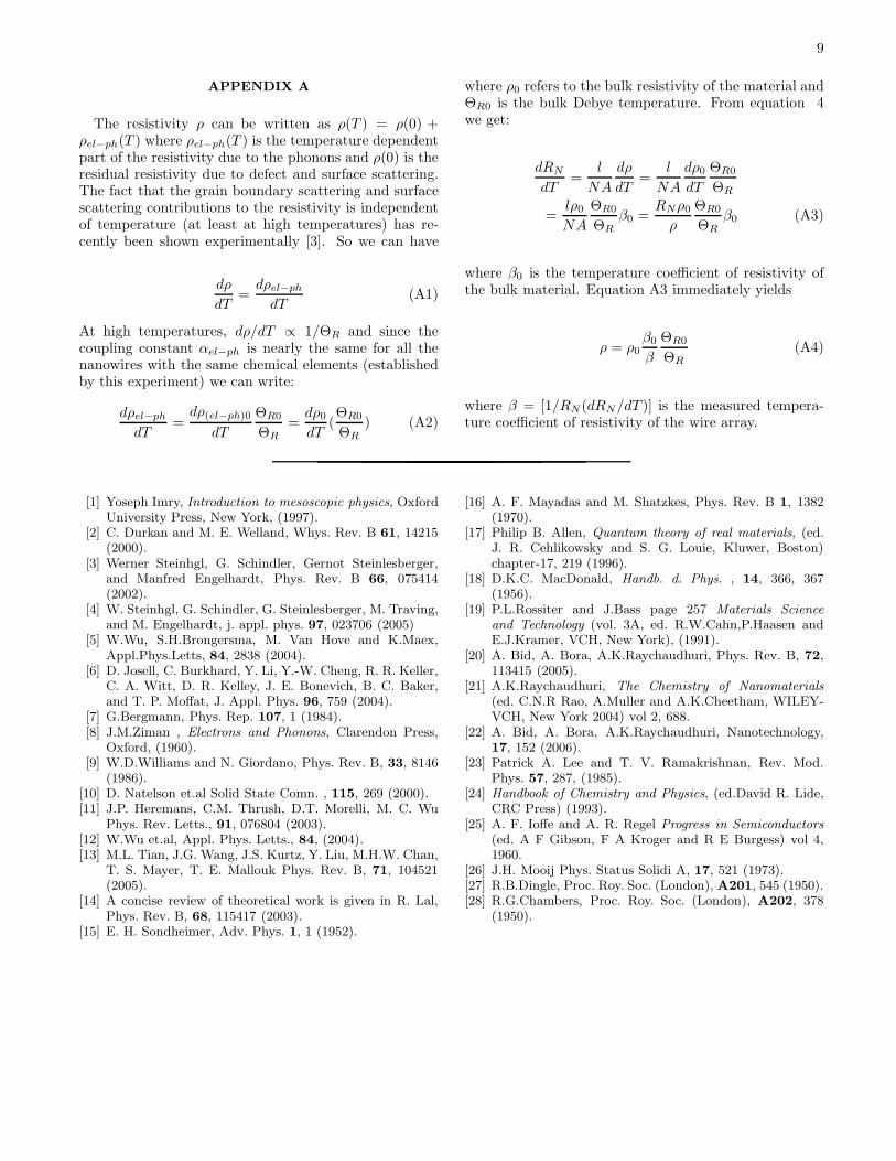
function of temperature for wires of different diameters.The value of the resistivity at 295K, the residual resistiv-ity as well as the mean-free path (lmfp) of the electronscalculated from the resistivity at T=295K are shown intable 2. For this calculation we assumed bulk electrondensity. In figure 10(a) we also plot the residual resistiv-ity ρ4.2K as well as the ρ295K as a function of d for theAg wires. (The bulk value of the resistivity of high purityAg (1.6 × 10⁻⁸Ωm) at 295K is shown as an arrow.) Wehave plotted the ratio lmfp/d at 295 K as a function ofd in figure 10(b). It clearly shows that in wires of smalldiameters the lmfp can be substantially larger than d andthat the ratio lmfp/d increases as d is reduced. For wiresof diameter 15 nm lmfp/d approaches a value 1.5. Wealso note that the value of kF l is significantly larger than1 thus justifying the applicability of the Bloch-Gruneisentheorem in these samples.
From table II as well as from figures 9 and 10 we cansee that there is a significant increase in the residual re-sistivity as the diameter of the wires is decreased. Theincrease is systematic. All wires have the same chemicalpurity and hence the enhancement of ρ4.2K on reductionof d is not due to impurity contribution. For wires in thediameter range that we are studying, the resistivity is ex-pected to increase with a decrease in the wire diameterdue to 2 probable reasons:
• As the mean free path of the electrons is now of theorder (and in some cases larger than) of the diam-
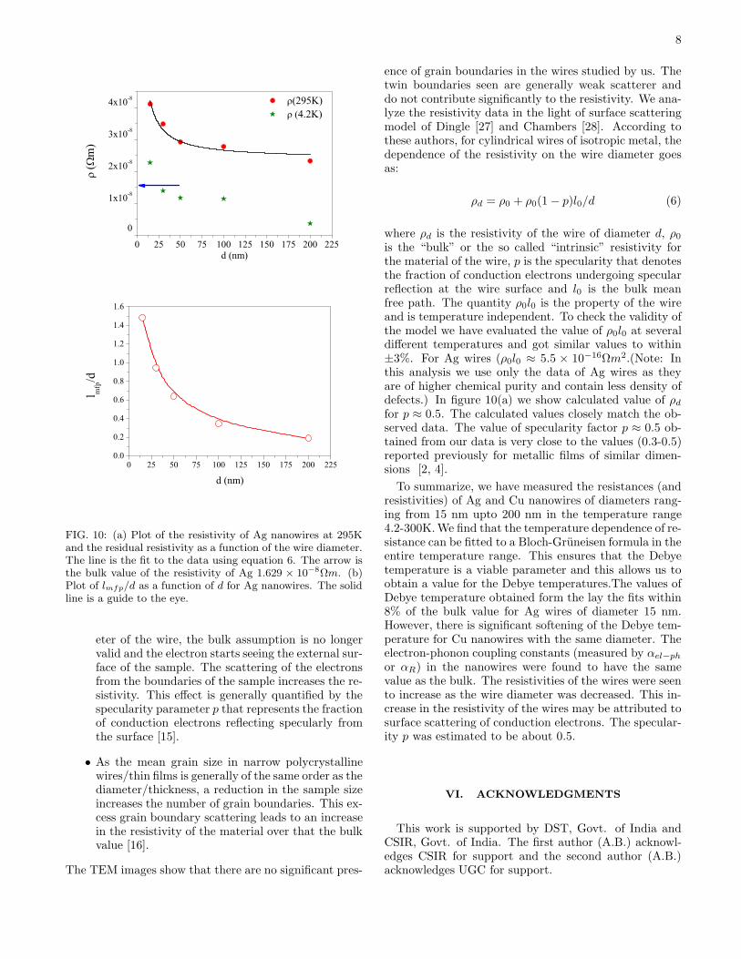
8
0 25 50 75 100 125 150 175 200 225
0
1x10⁻⁸
2x10⁻⁸
3x10⁻⁸
4x10⁻⁸ r(295K) r (4.2K)
r
(Wm
)
d (nm)
0 25 50 75 100 125 150 175 200 2250.0
0.2
0.4
0.6
0.8
1.0
1.2
1.4
1.6
l mfp
/d
d (nm)
FIG. 10: (a) Plot of the resistivity of Ag nanowires at 295Kand the residual resistivity as a function of the wire diameter.The line is the fit to the data using equation 6. The arrow isthe bulk value of the resistivity of Ag 1.629 × 10⁻⁸Ωm. (b)Plot of lmfp/d as a function of d for Ag nanowires. The solidline is a guide to the eye.
eter of the wire, the bulk assumption is no longervalid and the electron starts seeing the external sur-face of the sample. The scattering of the electronsfrom the boundaries of the sample increases the re-sistivity. This effect is generally quantified by thespecularity parameter p that represents the fractionof conduction electrons reflecting specularly fromthe surface [15].
• As the mean grain size in narrow polycrystallinewires/thin films is generally of the same order as thediameter/thickness, a reduction in the sample sizeincreases the number of grain boundaries. This ex-cess grain boundary scattering leads to an increasein the resistivity of the material over that the bulkvalue [16].
The TEM images show that there are no significant pres-
ence of grain boundaries in the wires studied by us. Thetwin boundaries seen are generally weak scatterer anddo not contribute significantly to the resistivity. We ana-lyze the resistivity data in the light of surface scatteringmodel of Dingle [27] and Chambers [28]. According tothese authors, for cylindrical wires of isotropic metal, thedependence of the resistivity on the wire diameter goesas:
ρd = ρ0 + ρ0(1 − p)l0/d (6)
where ρd is the resistivity of the wire of diameter d, ρ0
is the “bulk” or the so called “intrinsic” resistivity forthe material of the wire, p is the specularity that denotesthe fraction of conduction electrons undergoing specularreflection at the wire surface and l0 is the bulk meanfree path. The quantity ρ0l0 is the property of the wireand is temperature independent. To check the validity ofthe model we have evaluated the value of ρ0l0 at severaldifferent temperatures and got similar values to within±3%. For Ag wires (ρ0l0 ≈ 5.5 × 10⁻¹⁶Ωm2.(Note: Inthis analysis we use only the data of Ag wires as theyare of higher chemical purity and contain less density ofdefects.) In figure 10(a) we show calculated value of ρd
for p ≈ 0.5. The calculated values closely match the ob-served data. The value of specularity factor p ≈ 0.5 ob-tained from our data is very close to the values (0.3-0.5)reported previously for metallic films of similar dimen-sions [2, 4].
To summarize, we have measured the resistances (andresistivities) of Ag and Cu nanowires of diameters rang-ing from 15 nm upto 200 nm in the temperature range4.2-300K. We find that the temperature dependence of re-sistance can be fitted to a Bloch-Gruneisen formula in theentire temperature range. This ensures that the Debyetemperature is a viable parameter and this allows us toobtain a value for the Debye temperatures.The values ofDebye temperature obtained form the lay the fits within8% of the bulk value for Ag wires of diameter 15 nm.However, there is significant softening of the Debye tem-perature for Cu nanowires with the same diameter. Theelectron-phonon coupling constants (measured by αel−ph
or αR) in the nanowires were found to have the samevalue as the bulk. The resistivities of the wires were seento increase as the wire diameter was decreased. This in-crease in the resistivity of the wires may be attributed tosurface scattering of conduction electrons. The specular-ity p was estimated to be about 0.5.
VI. ACKNOWLEDGMENTS
This work is supported by DST, Govt. of India andCSIR, Govt. of India. The first author (A.B.) acknowl-edges CSIR for support and the second author (A.B.)acknowledges UGC for support.
9
APPENDIX A
The resistivity ρ can be written as ρ(T ) = ρ(0) +ρel−ph(T ) where ρel−ph(T ) is the temperature dependentpart of the resistivity due to the phonons and ρ(0) is theresidual resistivity due to defect and surface scattering.The fact that the grain boundary scattering and surfacescattering contributions to the resistivity is independentof temperature (at least at high temperatures) has re-cently been shown experimentally [3]. So we can have
dρ
dT=
dρel−ph
dT(A1)
At high temperatures, dρ/dT ∝ 1/ΘR and since thecoupling constant αel−ph is nearly the same for all thenanowires with the same chemical elements (establishedby this experiment) we can write:
dρel−ph
dT=
dρ(el−ph)0
dT
ΘR0
ΘR
=dρ0
dT(ΘR0
ΘR
) (A2)
where ρ0 refers to the bulk resistivity of the material andΘR0 is the bulk Debye temperature. From equation 4we get:
dRN
dT=
l
NA
dρ
dT=
l
NA
dρ0
dT
ΘR0
ΘR
=lρ0
NA
ΘR0
ΘR
β0 =RNρ0
ρ
ΘR0
ΘR
β0 (A3)
where β0 is the temperature coefficient of resistivity ofthe bulk material. Equation A3 immediately yields
ρ = ρ0β0
β
ΘR0
ΘR
(A4)
where β = [1/RN(dRN/dT )] is the measured tempera-ture coefficient of resistivity of the wire array.
[1] Yoseph Imry, Introduction to mesoscopic physics, OxfordUniversity Press, New York, (1997).
[2] C. Durkan and M. E. Welland, Whys. Rev. B 61, 14215(2000).
[3] Werner Steinhgl, G. Schindler, Gernot Steinlesberger,and Manfred Engelhardt, Phys. Rev. B 66, 075414(2002).
[4] W. Steinhgl, G. Schindler, G. Steinlesberger, M. Traving,and M. Engelhardt, j. appl. phys. 97, 023706 (2005)
[5] W.Wu, S.H.Brongersma, M. Van Hove and K.Maex,Appl.Phys.Letts, 84, 2838 (2004).
[6] D. Josell, C. Burkhard, Y. Li, Y.-W. Cheng, R. R. Keller,C. A. Witt, D. R. Kelley, J. E. Bonevich, B. C. Baker,and T. P. Moffat, J. Appl. Phys. 96, 759 (2004).
[7] G.Bergmann, Phys. Rep. 107, 1 (1984).[8] J.M.Ziman , Electrons and Phonons, Clarendon Press,
Oxford, (1960).[9] W.D.Williams and N. Giordano, Phys. Rev. B, 33, 8146
(1986).[10] D. Natelson et.al Solid State Comn. , 115, 269 (2000).[11] J.P. Heremans, C.M. Thrush, D.T. Morelli, M. C. Wu
Phys. Rev. Letts., 91, 076804 (2003).[12] W.Wu et.al, Appl. Phys. Letts., 84, (2004).[13] M.L. Tian, J.G. Wang, J.S. Kurtz, Y. Liu, M.H.W. Chan,
T. S. Mayer, T. E. Mallouk Phys. Rev. B, 71, 104521(2005).
[14] A concise review of theoretical work is given in R. Lal,Phys. Rev. B, 68, 115417 (2003).
[15] E. H. Sondheimer, Adv. Phys. 1, 1 (1952).
[16] A. F. Mayadas and M. Shatzkes, Phys. Rev. B 1, 1382(1970).
[17] Philip B. Allen, Quantum theory of real materials, (ed.J. R. Cehlikowsky and S. G. Louie, Kluwer, Boston)chapter-17, 219 (1996).
[18] D.K.C. MacDonald, Handb. d. Phys. , 14, 366, 367(1956).
[19] P.L.Rossiter and J.Bass page 257 Materials Science
and Technology (vol. 3A, ed. R.W.Cahn,P.Haasen andE.J.Kramer, VCH, New York), (1991).
[20] A. Bid, A. Bora, A.K.Raychaudhuri, Phys. Rev. B, 72,113415 (2005).
[21] A.K.Raychaudhuri, The Chemistry of Nanomaterials
(ed. C.N.R Rao, A.Muller and A.K.Cheetham, WILEY-VCH, New York 2004) vol 2, 688.
[22] A. Bid, A. Bora, A.K.Raychaudhuri, Nanotechnology,17, 152 (2006).
[23] Patrick A. Lee and T. V. Ramakrishnan, Rev. Mod.Phys. 57, 287, (1985).
[24] Handbook of Chemistry and Physics, (ed.David R. Lide,CRC Press) (1993).
[25] A. F. Ioffe and A. R. Regel Progress in Semiconductors
(ed. A F Gibson, F A Kroger and R E Burgess) vol 4,1960.
[26] J.H. Mooij Phys. Status Solidi A, 17, 521 (1973).[27] R.B.Dingle, Proc. Roy. Soc. (London), A201, 545 (1950).[28] R.G.Chambers, Proc. Roy. Soc. (London), A202, 378
(1950).


![The Gerasimov-Drell-Hearn Sum RuleHearn [2] according to Spiresas a function of time. One observes that until 1990 the interest in the GDH Sum Rule is essentially constant. This hesitant](https://static.fdocument.org/doc/165x107/60a60bb809c252409e4913ea/the-gerasimov-drell-hearn-sum-rule-hearn-2-according-to-spiresas-a-function-of.jpg)