01 Camera Ready_KAUST Repository
7
1 1 Abstract—We present a comprehensive electrical performance assessment of hafnium silicate (HfSiO x ) high-κ dielectric and titanium nitride (TiN) metal gate integrated FinFET-based complementary─metal─oxide semiconductor (CMOS) on flexible silicon-on-insulator (SOI). The devices were fabricated using state-of-the-art CMOS technology and then transformed into flexible form by using a CMOS-compatible mask-less deep reactive-ion etching (DRIE) technique. Mechanical out-of-plane stresses (compressive and tensile) were applied along and across the transistor channel lengths through a bending range of 0.5 to 5 cm radii for n-type and p-type FinFETs. Electrical measurements were carried out before and after bending, and all bending measurements were taken in the actual flexed (bent) state to avoid relaxation and stress recovery. Global stress from substrate bending affects the devices in different ways compared to the well-studied uniaxial/biaxial localized strain. The global stress is dependent on the type of channel charge carriers, the orientation of the bending axis, and the physical gate length of the device. We therefore outline useful insights on the design strategies of flexible FinFETs in future free-form electronic applications. Index Terms— Flexible, CMOS, FinFET, strain. I. INTRODUCTION THE Internet of Everything (IoE) envisions the connection of living beings (e.g. humans, plants, animals, and birds) and objects to the cloud, where vital signs, activity rates, and other aspects of daily life can be monitored and analyzed to inform decisions and improve lifestyles. In that sense, IoE devices require close proximity to the human body, fast decision making capability, and low heat dissipation. They must have low power consumption (dynamic and static), high performance, and flexibility. Subthreshold swing (SS) is a critical parameter to this end because it affects the switching speed of a transistor and its dynamic power consumption [1]. The nonplanar 3D architecture of a FinFET device also enables low-power operation and further scaling, to cope with Moore’s law [2, 3]. FinFET devices are already commercially available at higher technology nodes (22 and 14 nm). The international technology roadmap for semiconductors (ITRS) predicts a physical gate length requirement of 7 nm by 2025 [4]. Although such state-of-the-art CMOS electronics exhibit This publication is based upon work supported by the King Abdullah University of Science and Technology (KAUST) Office of Sponsored Research (OSR) under Award No. CRG-1-2012-HUS-008. We acknowledge Seneca J. Velling for proof reading this manuscript. All authors are with the Integrated Nanotechnology Lab and Integrated Disruptive Electronic Applications (IDEA) Lab, Electrical Engineering, Computer Electrical Mathematical Science and Engineering Division, King Abdullah University of Science and Technology, Thuwal 23955-6900, Saudi Arabia (e-mail: [email protected]). unparalleled advantages, they are rigid and bulky making them unsuitable for IoE applications. CMOS electronics thus need to be of freeform – physically flexible and stretchable. In this work, we applied various mechanical stresses through bending to the flexed FinFET devices to assess their suitability for flexible electronics applications, including IoE and wearable systems, where flexibility and high performance are essential features for components. We quantify and analyze the effect of out-of-plane stress on key performance metrics to provide insights into the integration feasibility of state-of-the-art CMOS devices with new emerging applications. II. EXPERIMENTAL We used SOI substrates with a 90 nm SOI layer (100) and a gate first approach. A summary of the main fabrication steps is depicted with a cross-section showing fin internal structure in Fig. 1(a-c), where the inset showing fins orientation. Fig. 1(d- f) show the main flexing steps to transform the rigid substrate into a 50-μm-thick flexible form. We used a Keithley 4200- SCS Semiconductor Characterization System on a manual SemiProbe probe station, as well as curved aluminum surfaces for device characterization (Fig. 1(g)). Bending was done along the fins (i.e., where the bending axis is parallel to the line connecting source and drain) and across the fins (i.e., where the bending axis is perpendicular to the fin length). III. RESULTS AND DISCUSSION A. Silicon’s Bending Ability and Limitations Fracture strength determines the overall mechanical stability of a flexible system. The three-point bending test is widely used to assess the fracture strength of a substrate. For silicon thicknesses below 100 μm, the linear elastic bending beam theory cannot provide an accurate estimation of fracture strength because thin substrates produce a nonlinear deflection-load relationship that is used to estimate fracture strength [8]. In 2015, Liu et al. introduced the large deflection theory of beam to account for this nonlinearity [9]. They offered important insights for theoretical limitations of flexible silicon thinner than 100 μm. Furthermore, based on the application’s required bending radius, the thickness of the flexible silicon substrate must be adjusted such that the applied stress is determined as = ɛ(1) Where is the stress in Pascals, Y is Young’s modulus, and ɛ is the nominal strain, which can be calculated as Out-of-Plane Strain Effects on Physically Flexible FinFET CMOS Mohamed T. Ghoneim, Student Member, IEEE, Nasir Alfaraj, Student Member, IEEE, Galo A. Torres-Sevilla, Student Member, IEEE, Hossain M. Fahad, Member, IEEE, and Muhammad M. Hussain, Senior Member, IEEE
-
Upload
mohamed-ghoneim -
Category
Documents
-
view
139 -
download
0
Transcript of 01 Camera Ready_KAUST Repository
1
1
Abstract—We present a comprehensive electrical performance
assessment of hafnium silicate (HfSiOx) high-κ dielectric and
titanium nitride (TiN) metal gate integrated FinFET-based
complementary─metal─oxide semiconductor (CMOS) on flexible
silicon-on-insulator (SOI). The devices were fabricated using
state-of-the-art CMOS technology and then transformed into
flexible form by using a CMOS-compatible mask-less deep
reactive-ion etching (DRIE) technique. Mechanical out-of-plane
stresses (compressive and tensile) were applied along and across
the transistor channel lengths through a bending range of 0.5 to 5
cm radii for n-type and p-type FinFETs. Electrical measurements
were carried out before and after bending, and all bending
measurements were taken in the actual flexed (bent) state to
avoid relaxation and stress recovery. Global stress from substrate
bending affects the devices in different ways compared to the
well-studied uniaxial/biaxial localized strain. The global stress is
dependent on the type of channel charge carriers, the orientation
of the bending axis, and the physical gate length of the device. We
therefore outline useful insights on the design strategies of
flexible FinFETs in future free-form electronic applications.
Index Terms— Flexible, CMOS, FinFET, strain.
I. INTRODUCTION
THE Internet of Everything (IoE) envisions the connection of
living beings (e.g. humans, plants, animals, and birds) and
objects to the cloud, where vital signs, activity rates, and other
aspects of daily life can be monitored and analyzed to inform
decisions and improve lifestyles. In that sense, IoE devices
require close proximity to the human body, fast decision
making capability, and low heat dissipation. They must have
low power consumption (dynamic and static), high
performance, and flexibility. Subthreshold swing (SS) is a
critical parameter to this end because it affects the switching
speed of a transistor and its dynamic power consumption [1].
The nonplanar 3D architecture of a FinFET device also
enables low-power operation and further scaling, to cope with
Moore’s law [2, 3]. FinFET devices are already commercially
available at higher technology nodes (22 and 14 nm). The
international technology roadmap for semiconductors (ITRS)
predicts a physical gate length requirement of 7 nm by 2025
[4]. Although such state-of-the-art CMOS electronics exhibit
This publication is based upon work supported by the King Abdullah
University of Science and Technology (KAUST) Office of Sponsored
Research (OSR) under Award No. CRG-1-2012-HUS-008. We acknowledge Seneca J. Velling for proof reading this manuscript. All authors are with the
Integrated Nanotechnology Lab and Integrated Disruptive Electronic
Applications (IDEA) Lab, Electrical Engineering, Computer Electrical Mathematical Science and Engineering Division, King Abdullah University of
Science and Technology, Thuwal 23955-6900, Saudi Arabia (e-mail:
unparalleled advantages, they are rigid and bulky making them
unsuitable for IoE applications. CMOS electronics thus need
to be of freeform – physically flexible and stretchable.
In this work, we applied various mechanical stresses
through bending to the flexed FinFET devices to assess their
suitability for flexible electronics applications, including IoE
and wearable systems, where flexibility and high performance
are essential features for components. We quantify and
analyze the effect of out-of-plane stress on key performance
metrics to provide insights into the integration feasibility of
state-of-the-art CMOS devices with new emerging
applications.
II. EXPERIMENTAL
We used SOI substrates with a 90 nm SOI layer (100) and a
gate first approach. A summary of the main fabrication steps is
depicted with a cross-section showing fin internal structure in
Fig. 1(a-c), where the inset showing fins orientation. Fig. 1(d-
f) show the main flexing steps to transform the rigid substrate
into a 50-μm-thick flexible form. We used a Keithley 4200-
SCS Semiconductor Characterization System on a manual
SemiProbe probe station, as well as curved aluminum surfaces
for device characterization (Fig. 1(g)). Bending was done
along the fins (i.e., where the bending axis is parallel to the
line connecting source and drain) and across the fins (i.e.,
where the bending axis is perpendicular to the fin length).
III. RESULTS AND DISCUSSION
A. Silicon’s Bending Ability and Limitations
Fracture strength determines the overall mechanical
stability of a flexible system. The three-point bending test is
widely used to assess the fracture strength of a substrate. For
silicon thicknesses below 100 μm, the linear elastic bending
beam theory cannot provide an accurate estimation of fracture
strength because thin substrates produce a nonlinear
deflection-load relationship that is used to estimate fracture
strength [8].
In 2015, Liu et al. introduced the large deflection theory of
beam to account for this nonlinearity [9]. They offered
important insights for theoretical limitations of flexible silicon
thinner than 100 μm. Furthermore, based on the application’s
required bending radius, the thickness of the flexible silicon
substrate must be adjusted such that the applied stress is
determined as
𝜎 = 𝑌ɛ(1) Where 𝜎 is the stress in Pascals, Y is Young’s modulus, and ɛ
is the nominal strain, which can be calculated as
Out-of-Plane Strain Effects on Physically Flexible
FinFET CMOS Mohamed T. Ghoneim, Student Member, IEEE, Nasir Alfaraj, Student Member, IEEE, Galo A. Torres-Sevilla,
Student Member, IEEE, Hossain M. Fahad, Member, IEEE, and Muhammad M. Hussain, Senior Member, IEEE
2
ɛ𝑛𝑜𝑚𝑖𝑛𝑎𝑙 =𝑡
2𝑅 (2)
Where 𝑡 is the substrate thickness and 𝑅 is the bending radius.
The applied stress needs to be lower than the fracture stress
for mechanical integrity. Reference [9] showed that for a 50-
μm-thick silicon fabric, the fracture stress is about 1.1 GPa.
Substituting a (100) silicon Young’s modulus of 128 GPa [10]
in Equation (1), and the resulting strain value from Equation
(2), we obtain a minimum bending radius for the 50-μm-thick
flexible silicon fabric of approximately 3 mm, which
decreases with a decreasing thickness. Therefore, a plain
flexible silicon substrate that is 50-μm-thick or thinner with a
bending radius of more than 3 mm will safely operate below
the fracture stress level. We emphasize that these results are
for a bare silicon substrate with no additive layers or patterns
for devices. Therefore, based on material properties, substrate
thickness, and the bending radius necessary for a specific
application, we can determine the most suitable approach and
material system for fabricating a thin substrate. These results
identify important boundary limitations and guarantee that a
bending of 0.5 cm is reasonably far from fracture stress
regime. In most cases where flexible electronics are required
to wrap around curvilinear objects, such as covering a
fingertip or an arm, a bending radius of 3 mm would suffice.
Moreover, continuing to reduce the substrate’s thickness is
another option that would enable us to decrease the bending
radii and achieve a similar nominal strain corresponding to
stress values below the fracture limit. Nonetheless, polymeric
electronics exhibit better flexibility and might be a more
feasible option for extreme applications that require folding of
the substrate. Sekitani et al. demonstrated ultra-flexibility
using polymeric substrates and Pentacene semiconductor-
based organic-thin-film transistors (OTFT) that can bend at
100 µm radius for various applications [11].
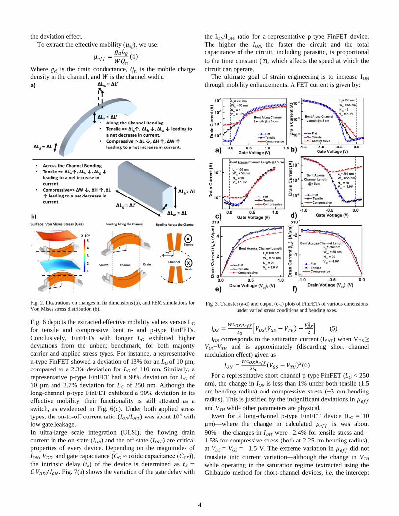
B. Effect of Bending Axis Orientation, Stress Type,
Carrier Type on FinFET Performance
Empirical analysis of the effects of bending direction and
bending axis orientation on the dimensions of the fins,
representing the carrier channels, should provide useful
insights into the feasibility of the integration of state-of-the-art
CMOS devices into the aforementioned IoE applications.
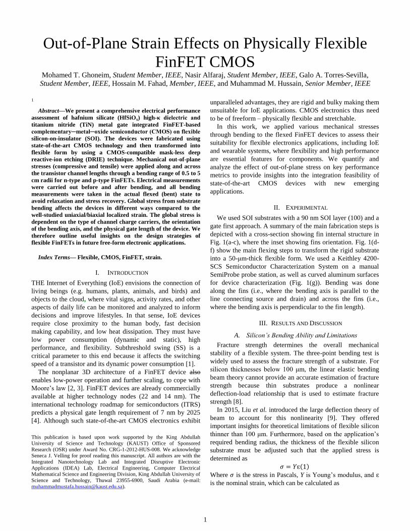
Silicon’s elastic modulus (128 GPa for (100) silicon) allows us
to relate the (100) silicon Poisson’s ratio of 0.17 [12] to the
change in dimension through the following basic equation
𝑣 ≈∆𝐿′
∆𝐿 (3)
Where ∆𝐿′ is transverse strain and ∆L is the axial strain, as
shown in Fig. 2(a). Fig. 2(b) shows the finite element method
(FEM) simulation results for surface tensile and compressive
stresses, anticipating that compressive stress has a greater
impact on device behavior (nearly doubling applied stress at
the surface containing the devices), while illustrating the two
bending conditions (across and along the channel). Fig. 3
shows the effect of compressive and tensile stresses on the
saturation transfer I━V characteristics of a sub-micron
physical gate length (Lg) n-type and p-type FinFETs bent at ±3
cm along the channel (Fig. 3(a-b)), and FinFETs bent at ±5
cm across the channel (Fig. 3(c-d)), corresponding to 0.08 %
and 0.05% nominal strain, respectively. The measurements
confirm that compressive stress always has a more
pronounced effect for both devices━for different channel
carriers types and for both bending axes (i.e., along and across
the channel). We note the change of bending dimensions
analysis by the output I━V characteristics curves, which
showcase the pattern on a linear scale (Fig. 3(e-f)). Based on
changes in the fin/channel dimensions depicted in Fig. 2(a),
the pattern is expected. However, this pattern was not
meticulously followed in the case of along-the-channel
bending, indicating that the variation is better explained as an
anomaly in behavior within a specific variation range than a
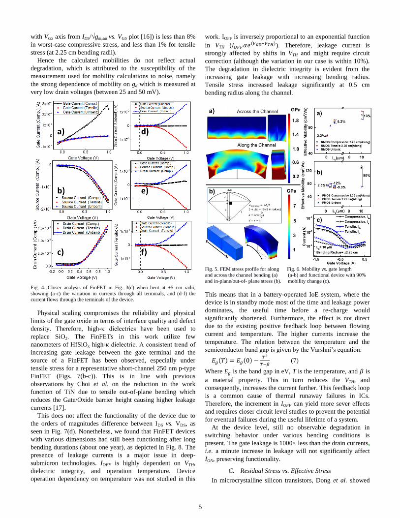
consistent trend. Fig. 4(a-c) show the current flowing between
the three terminals (Source/Drain/Gate) in the FinFET
depicted in Fig. 3 (c) on a linear scale. In unbent and tensile
stress cases, as the electric field in the channel becomes
stronger, the gate leakage is almost constant and current flows
between source and drain prominently. On the other hand, in
case of compressive stress, the magnitude of both subthreshold
leakage in the channel and gate leakage increase, and as the
electric field between the gate and the channel increases, the
gate leakage current linearly increases. This effect is better
expressed in the subthreshold regime due to lower current
levels between the source and drain, where gate leakage is of
comparable magnitude. In all cases, the vector sum of currents
is zero, except where the individual components are flowing,
indicative of a compromised gate dielectric integrity under
compressive stressing. For instance, Fig. 4(d-f) show that for
unbent and tensile stress, the off current (subthreshold channel
current and gate leakage) is due to current flowing from Drain
Fig. 1. Fabrication flow (a-f) and characterization setup (g) of flexible FinFET.
3
(VDD) into Source (ground) and Gate (ground) terminals,
remaining nearly constant as Gate voltage increases until
switching occurs. On the other hand, under compressive stress,
IOFF is initially higher and gate leakage continues to increase
linearly with increasing Gate voltage, indicating conduction
through the gate dielectric as current now flows from Gate and
Drain into the Source in subthreshold regime and continues
even after the transistor is switched ON. This confirms that the
effect results from a compromised dielectric integrity caused
by compressive stress.
Localized strain enhancement in CMOS transistors has been
extensively studied for decades [13], with the assumption that
different carriers will respond to stress differently. Wesler et
al. used energy band diagrams to explain the different
responses to stress with respect to carrier types [14]. For
instance, in the suggested SiO2/Si/Si0.7Ge0.3 strained structure,
a barrier hole well in the valence band corresponds to a
surface electron well in the conduction band. The strained
silicon surface energy band structure is similar to the bent
FinFETs case, where the stress gradient along the silicon
thickness due to bending induces a strain effect, rather than the
SiGe layer, influencing the effective masses (m*) of charge
carriers due to the deformations in the constrained/stretched
energy (E) bands (𝑚∗𝛼 (𝑑2𝐸
𝑑𝐾2)−1
, where K is proportional to
crystal momentum). However, due to band bending in
different directions, tensile and compressive strains should
form different barrier and surface well structures, depending
on carrier type. This affects the transport properties especially
at the edges of the channel (or fins) where lateral stress values
are relatively higher and extra surface and barrier wells for
carriers are likely to form. Oppositely charged free carriers
behave differently depending on the bending axis (Fig. 3).
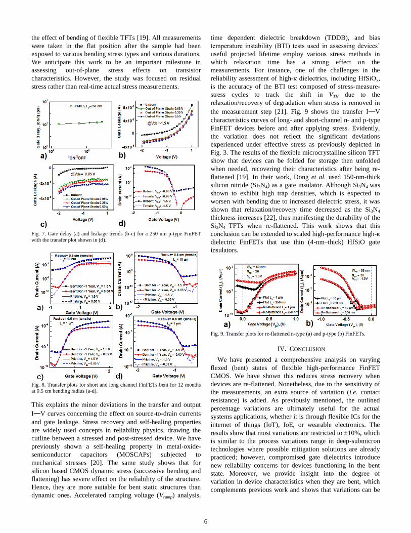
Further FEM analysis, as represented by Fig. 5(a), shows a
two-dimensional stress distribution in a fin bent across the
channel and along the channel. Devices with larger
dimensions would show similar stress distribution. The critical
point would be for further scaled-down devices where the
higher stress regions merge to form different stress patterns,
which might stress the whole channel and lead to different
behavior. Comparing the two stress profiles, it is clear that
bending across the channel leads to different stress distribution
than bending along the channel. As can be deduced from the
results shown in Fig. 3, electrons are more sensitive to stress
when the channel is bent along its length, while holes are more
sensitive when the bending axis is perpendicular to the
channel length. Because CMOS-based technology utilizes
both n- and p-type field-effect transistors (FETs) on the same
wafer, the assessed degradation should be the worst-case
scenario for both of the two channel types. Furthermore,
localized stress due to SiGe source and drain has historically
been used to strain the channel and enhance mobility. On the
other hand, a dissimilar effect takes place in this study. This is
because empirical stress imposed by out-of-plane bending
causes a different stress distribution profile and different
magnitudes compared to localized stress when both are
exposed to same strain values (Fig. 5(b)). The inset in Fig.
5(b) shows the calculation of the displacement required for
specific strain and the resulting stress profiles for out-of-plane
and in-plane fins, stressed at the same strain values. Using
equations (1-2), the stress regime for 0.5 to 5 cm bending radii
is 80 to 800 MPa, corresponding to an intermediate stress
range relatively lower than that used in strained silicon to
engineer mobility enhancements [15]. Still there were cases of
mobility enhancements for long-channel devices flexed along
the channel, but due to the complexity of the testing setup and
sources of variation while contacting the devices, the
conclusion would be an anomaly within ±5% for short-
channel devices. Other key switching properties are
summarized in Table I for short-channel FinFETs bent at ±5
cm bending radius.
Table I
Key switching properties of short-channel FinFETs under out-of-
plane stress due to ±5 cm bending radius
Parameter Method %
change
SS min(∆𝑉𝐺𝑆 𝑙𝑜𝑔(𝐼𝐷𝑆1 𝐼𝐷𝑆2))⁄⁄ ~10%
VTH 𝐼𝐷𝑆/𝑔𝑚 − 𝑉𝐺𝑆|@max𝑔𝑚 ~10%
DIBL (𝑉𝑇𝐻,𝑠𝑎𝑡 − 𝑉𝑇𝐻,𝑙𝑖𝑛) (𝑉𝐷𝐷 − 𝑉𝐷𝑆,𝑙𝑜𝑤)⁄ ±50%
𝒈𝒎,𝒎𝒂𝒙 𝜕𝐼𝐷𝑆 𝜕𝑉𝐺𝑆⁄ -40%
ION/IOFF Ratio 𝐼𝑂𝑁 @𝑉𝐷𝑆 = 𝑉𝐺𝑆 = 𝑉𝐷𝐷
𝐼𝑂𝐹𝐹 @𝑉𝐷𝑆 = 𝑉𝐷𝐷, 𝑉𝐺𝑆 = 0 V
~33%
The large variation in the drain-induced barrier lowering
(DIBL) implies that the devices suffered from significant
threshold voltage (VTH) shifts when functioning in the
saturation regime. An increment under compressive stress
implies that the device suffers higher leakage currents due to a
relatively larger reduction in VTH. A decrease in DIBL under
tensile stress would lead to a device with relatively larger VTH
than designed, and, consequently, lower overdrive voltage
(VDD–VTH, where VDD is the supply voltage) and on-state
currents (ION). The decrease in the peak transconductance (gm)
would degrade the performance of a transistor device while
operating as an amplifier, because the gain of an amplifier is
proportional to the transconductance of the device. Ideally,
ICs are designed to tolerate 10% deviation in circuit
parameters. Therefore, for anomalies greater than 10%,
serious considerations are essential when integrating such
high-performance devices in flexible ICs that are intended to
function properly under various bending conditions. This can
be mitigated by redundant compensation elements to adjust
the parameters. Current design for yield in deep-submicron
technologies already uses similar techniques to comply with
3σ and 6σ standards (σ measures variability), accommodating
process variations for extremely scaled emerging nodes. For
instance, adding a backup transistor connected in parallel
when needed to enhance the circuit current as the original
transistor experiences increased VTH and lower current. The
observed trend for increased gate leakage with bending can be
utilized to sense the leakage current and determine the
corresponding parameter deviation, allowing us to make
dynamic decisions to engage added components and correct
4
the deviation effect.
To extract the effective mobility (µeff), we use:
µ𝑒𝑓𝑓 =𝑔𝑑𝐿𝑔
𝑊𝑄𝑛(4)
Where 𝑔𝑑 is the drain conductance, 𝑄𝑛 is the mobile charge
density in the channel, and 𝑊 is the channel width.
Fig. 2. Illustrations on changes in fin dimensions (a), and FEM simulations for
Von Mises stress distribution (b).
Fig. 6 depicts the extracted effective mobility values versus LG
for tensile and compressive bent n- and p-type FinFETs.
Conclusively, FinFETs with longer LG exhibited higher
deviations from the unbent benchmark, for both majority
carrier and applied stress types. For instance, a representative
n-type FinFET showed a deviation of 13% for an LG of 10 µm,
compared to a 2.3% deviation for LG of 110 nm. Similarly, a
representative p-type FinFET had a 90% deviation for LG of
10 µm and 2.7% deviation for LG of 250 nm. Although the
long-channel p-type FinFET exhibited a 90% deviation in its
effective mobility, their functionality is still attested as a
switch, as evidenced in Fig. 6(c). Under both applied stress
types, the on-to-off current ratio (ION/IOFF) was about 103 with
low gate leakage.
In ultra-large scale integration (ULSI), the flowing drain
current in the on-state (ION) and the off-state (IOFF) are critical
properties of every device. Depending on the magnitudes of
ION, VDD, and gate capacitance (CG ≈ oxide capacitance (COX)),
the intrinsic delay (td) of the device is determined as 𝑡𝑑 =𝐶 𝑉𝐷𝐷 𝐼𝑂𝑁⁄ . Fig. 7(a) shows the variation of the gate delay with
the ION/IOFF ratio for a representative p-type FinFET device.
The higher the ION, the faster the circuit and the total
capacitance of the circuit, including parasitic, is proportional
to the time constant (τ), which affects the speed at which the
circuit can operate.
The ultimate goal of strain engineering is to increase ION
through mobility enhancements. A FET current is given by:
Fig. 3. Transfer (a-d) and output (e-f) plots of FinFETs of various dimensions
under varied stress conditions and bending axes.
𝐼𝐷𝑆 =𝑊𝐶𝑂𝑋𝜇𝑒𝑓𝑓
𝐿𝐺[𝑉𝐷𝑆(𝑉𝐺𝑆 − 𝑉𝑇𝐻) −
𝑉𝐷𝑆2
2] (5)
ION corresponds to the saturation current (ISAT) when VDS ≥
VGS−VTH and is approximately (discarding short channel
modulation effect) given as
𝐼𝑂𝑁 =𝑊𝐶𝑂𝑋𝜇𝑒𝑓𝑓
2𝐿𝐺(𝑉𝐺𝑆 − 𝑉𝑇𝐻)
2(6)
For a representative short-channel p-type FinFET (LG < 250
nm), the change in ION is less than 1% under both tensile (1.5
cm bending radius) and compressive stress (−3 cm bending
radius). This is justified by the insignificant deviations in 𝜇𝑒𝑓𝑓
and VTH while other parameters are physical.
Even for a long-channel p-type FinFET device (LG = 10
μm)—where the change in calculated 𝜇𝑒𝑓𝑓 is was about
90%—the changes in ISAT were –2.4% for tensile stress and –
1.5% for compressive stress (both at 2.25 cm bending radius),
at VDS = VGS = –1.5 V. The extreme variation in 𝜇𝑒𝑓𝑓 did not
translate into current variation—although the change in VTH
while operating in the saturation regime (extracted using the
Ghibaudo method for short-channel devices, i.e. the intercept
5
with VGS axis from IDS/√gm,sat vs. VGS plot [16]) is less than 8%
in worst-case compressive stress, and less than 1% for tensile
stress (at 2.25 cm bending radii).
Hence the calculated mobilities do not reflect actual
degradation, which is attributed to the susceptibility of the
measurement used for mobility calculations to noise, namely
the strong dependence of mobility on gd which is measured at
very low drain voltages (between 25 and 50 mV).
Fig. 4. Closer analysis of FinFET in Fig. 3(c) when bent at ±5 cm radii,
showing (a-c) the variation in currents through all terminals, and (d-f) the current flows through the terminals of the device.
Physical scaling compromises the reliability and physical
limits of the gate oxide in terms of interface quality and defect
density. Therefore, high-κ dielectrics have been used to
replace SiO2. The FinFETs in this work utilize few
nanometers of HfSiOx high-κ dielectric. A consistent trend of
increasing gate leakage between the gate terminal and the
source of a FinFET has been observed, especially under
tensile stress for a representative short-channel 250 nm p-type
FinFET (Figs. 7(b-c)). This is in line with previous
observations by Choi et al. on the reduction in the work
function of TiN due to tensile out-of-plane bending which
reduces the Gate/Oxide barrier height causing higher leakage
currents [17].
This does not affect the functionality of the device due to
the orders of magnitudes difference between IDS vs. VDS, as
seen in Fig. 7(d). Nonetheless, we found that FinFET devices
with various dimensions had still been functioning after long
bending durations (about one year), as depicted in Fig. 8. The
presence of leakage currents is a major issue in deep-
submicron technologies. IOFF is highly dependent on VTH,
dielectric integrity, and operation temperature. Device
operation dependency on temperature was not studied in this
work. IOFF is inversely proportional to an exponential function
in VTH (𝐼𝑂𝐹𝐹𝛼𝑒(𝑉𝐺𝑆−𝑉𝑇𝐻)). Therefore, leakage current is
strongly affected by shifts in VTH and might require circuit
correction (although the variation in our case is within 10%).
The degradation in dielectric integrity is evident from the
increasing gate leakage with increasing bending radius.
Tensile stress increased leakage significantly at 0.5 cm
bending radius along the channel.
Fig. 5. FEM stress profile for along Fig. 6. Mobility vs. gate length
and across the channel bending (a) (a-b) and functional device with 90%
and in-plane/out-of- plane stress (b). mobility change (c).
This means that in a battery-operated IoE system, where the
device is in standby mode most of the time and leakage power
dominates, the useful time before a re-charge would
significantly shortened. Furthermore, the effect is not direct
due to the existing positive feedback loop between flowing
current and temperature. The higher currents increase the
temperature. The relation between the temperature and the
semiconductor band gap is given by the Varshni’s equation:
𝐸𝑔(𝑇) = 𝐸𝑔(0) −𝑇2
𝑇−𝛽 (7)
Where 𝐸𝑔 is the band gap in eV, T is the temperature, and 𝛽 is
a material property. This in turn reduces the VTH, and
consequently, increases the current further. This feedback loop
is a common cause of thermal runaway failures in ICs.
Therefore, the increment in IOFF can yield more sever effects
and requires closer circuit level studies to prevent the potential
for eventual failures during the useful lifetime of a system.
At the device level, still no observable degradation in
switching behavior under various bending conditions is
present. The gate leakage is 1000× less than the drain currents,
i.e. a minute increase in leakage will not significantly affect
ION, preserving functionality.
C. Residual Stress vs. Effective Stress
In microcrystalline silicon transistors, Dong et al. showed
6
the effect of bending of flexible TFTs [19]. All measurements
were taken in the flat position after the sample had been
exposed to various bending stress types and various durations.
We anticipate this work to be an important milestone in
assessing out-of-plane stress effects on transistor
characteristics. However, the study was focused on residual
stress rather than real-time actual stress measurements.
Fig. 7. Gate delay (a) and leakage trends (b-c) for a 250 nm p-type FinFET
with the transfer plot shown in (d).
Fig. 8. Transfer plots for short and long channel FinFETs bent for 12 months
at 0.5 cm bending radius (a-d).
This explains the minor deviations in the transfer and output
I━V curves concerning the effect on source-to-drain currents
and gate leakage. Stress recovery and self-healing properties
are widely used concepts in reliability physics, drawing the
cutline between a stressed and post-stressed device. We have
previously shown a self-healing property in metal-oxide-
semiconductor capacitors (MOSCAPs) subjected to
mechanical stresses [20]. The same study shows that for
silicon based CMOS dynamic stress (successive bending and
flattening) has severe effect on the reliability of the structure.
Hence, they are more suitable for bent static structures than
dynamic ones. Accelerated ramping voltage (Vramp) analysis,
time dependent dielectric breakdown (TDDB), and bias
temperature instability (BTI) tests used in assessing devices’
useful projected lifetime employ various stress methods in
which relaxation time has a strong effect on the
measurements. For instance, one of the challenges in the
reliability assessment of high-κ dielectrics, including HfSiOx,
is the accuracy of the BTI test composed of stress-measure-
stress cycles to track the shift in VTH due to the
relaxation/recovery of degradation when stress is removed in
the measurement step [21]. Fig. 9 shows the transfer I━V
characteristics curves of long- and short-channel n- and p-type
FinFET devices before and after applying stress. Evidently,
the variation does not reflect the significant deviations
experienced under effective stress as previously depicted in
Fig. 3. The results of the flexible microcrystalline silicon TFT
show that devices can be folded for storage then unfolded
when needed, recovering their characteristics after being re-
flattened [19]. In their work, Dong et al. used 150-nm-thick
silicon nitride (Si3N4) as a gate insulator. Although Si3N4 was
shown to exhibit high trap densities, which is expected to
worsen with bending due to increased dielectric stress, it was
shown that relaxation/recovery time decreased as the Si3N4
thickness increases [22], thus manifesting the durability of the
Si3N4 TFTs when re-flattened. This work shows that this
conclusion can be extended to scaled high-performance high-κ
dielectric FinFETs that use thin (4-nm–thick) HfSiO gate
insulators.
Fig. 9. Transfer plots for re-flattened n-type (a) and p-type (b) FinFETs.
IV. CONCLUSION
We have presented a comprehensive analysis on varying
flexed (bent) states of flexible high-performance FinFET
CMOS. We have shown this reduces stress recovery when
devices are re-flattened. Nonetheless, due to the sensitivity of
the measurements, an extra source of variation (i.e. contact
resistance) is added. As previously mentioned, the outlined
percentage variations are ultimately useful for the actual
systems applications, whether it is through flexible ICs for the
internet of things (IoT), IoE, or wearable electronics. The
results show that most variations are restricted to ±10%, which
is similar to the process variations range in deep-submicron
technologies where possible mitigation solutions are already
practiced; however, compromised gate dielectrics introduce
new reliability concerns for devices functioning in the bent
state. Moreover, we provide insight into the degree of
variation in device characteristics when they are bent, which
complements previous work and shows that variations can be
7
mitigated to render the devices suitable for performing while
bent as well as when flattened. This work presents the
possibility of adding the flexing ability to industry-grade
FinFETs without sacrificing functionality and highlights the
various effects that out-of-plane bending has on these devices.
REFERENCES
[1] J. Zhang, M. De Marchi, P.-E. Gaillardon, and G. De Micheli, "A
Schottky-Barrier Silicon FinFET with 6.0 mV/dec Subthreshold Slope over 5 Decades of Current," in Proc. IEEE Int. Electron Devices
Meeting, 2014, No. EPFL-CONF-201905.
[2] G. Moore. (1965). Cramming More Components Onto Integrated Circuits, Electronics. Proc. IEEE [Online]. 86(1), pp. 82-85. Available: http://ieeexplore.ieee.org/xpls/abs_all.jsp?arnumber=658762
[3] E. Yu, L. Chang, S. Ahmed, H. Wang, S. Bell, C. Y. Yang, C. Tabery, C. Ho, Q. Xiang, T. J. King, and J. Bokor, , "FinFET scaling to 10 nm
gate length," in Proc. IEEE Int. Electron Devices Meeting, 2002, pp.
251-254. [4] The International Technology Roadmap for Semiconductors, "Table
ORTC-1: ITRS Technology Trend Targets," Semicond. Ind. Assoc.,
Washington, DC, USA, 2013.
[5] T.-i. Kim, Y. H. Jung, H.-J Chung, K. J. Yu, N. Ahmed, C. J. Corcoran,
J. S. Park, S. H. Jin, and J. A. Rogers. (2013). Deterministic assembly of
releasable single crystal silicon-metal oxide field-effect devices formed from bulk wafers. Appl. Phys. Lett. [Online]. 102 (18), pp. 182104.
Available:
http://scitation.aip.org/content/aip/journal/apl/102/18/10.1063/1.4804139
[6] S. A. Stauth and B. A. Parviz. (2006). Self-assembled single-crystal
silicon circuits on plastic. Proc. Natl. Acad. Sci. [Online]. 103(28), pp. 13922-13927. Available: http://www.pnas.org/content/103/38/13922.full
[7] G. A. T. Sevilla, J. P. Rojas, H. M. Fahad, A. M. Hussain, R. Ghanem,
C. E. Smith, and M. M. Hussain. (2014, May). Flexible and Transparent
Silicon‐on‐Polymer Based Sub‐20 nm Non‐planar 3D FinFET for Brain‐Architecture Inspired Computation. Adv. Mater. [Online]. 26(18), pp.
2794-2799. Available:
http://onlinelibrary.wiley.com/doi/10.1002/adma.201305309/abstract [8] J. Wu, C. Huang, and C. Liao, "Fracture strength characterization and
failure analysis of silicon dies," Microelectron. Rel., vol. 43, no. 2, p.
269-277, Feb. 2003. [Online]. Available: http://www.sciencedirect.com/science/article/pii/S0026271402003141
[9] Z. Liu, Y. Huang, L. Xiao, P. Tang, and Z. Yin. (2015, Mar.). Nonlinear
characteristics in fracture strength test of ultrathin silicon die. Semicond. Sci. Techol. [Online]. 30(4), pp. 045005. Available:
http://iopscience.iop.org/article/10.1088/0268-
1242/30/4/045005/meta;jsessionid=F652D4CD866BA99D001F1C319E0B7BAB.ip-10-40-2-108
[10] E. J. Boyd and D. Uttamchandani. (2012, Feb.). Measurement of the
anisotropy of young's modulus in single-crystal silicon. J. Microelectromech. Syst. [Online]. 21(1), pp. 243-249. Avialable:
http://ieeexplore.ieee.org/stamp/stamp.jsp?arnumber=6093930
[11] T. Sekitani, U. Zschieschang, H. Klauk, and T. Someya. (2010, Nov.). Flexible organic transistors and circuits with extreme bending stability.
Nat. Mater.[Online]. 9, pp. 1015-1022. Available:
http://www.nature.com/nmat/journal/v9/n12/abs/nmat2896.html [12] J. Dolbow and M. Gosz. (1996, Aug.). Effect of out-of-plane properties
of a polyimide film on the stress fields in microelectronic structures.
Mech. Mater. [Online]. 23(4), pp. 311-321. Available:
http://www.sciencedirect.com/science/article/pii/016766369600021X
[13] S. E. Thompson, M. Armstrong, C. Auth, M. Alavi, M. Buehler, R. Chau, S. Cea, T. Ghani, G. Glass, T. Hoffman, and C. H. Jan. (2004,
Nov.). A 90-nm logic technology featuring strained-silicon. IEEE Trans.
Electron Devices [Online]. 51(11), pp. 1790-1797. Available: http://ieeexplore.ieee.org/xpls/abs_all.jsp?arnumber=1347396
[14] J. Welser, J. Hoyt, and J. Gibbons, "NMOS and PMOS transistors
fabricated in strained silicon/relaxed silicon-germanium structures," in Proc. IEEE Int. Electron Devices Meeting, 1992, pp. 1000-1002.
[15] K. Rim, J. Chu, H. Chen, K. A. Jenkins, T. Kanarsky, K. Lee, A.
Mocuta, H. Zhu, R. Roy, J. Newbury, and J. Ott,., "Characteristics and device design of sub-100 nm strained Si N-and PMOSFETs," in Symp.
VLSI Technol., Dig. Tech. Pap., 2002, pp. 98-99.
[16] L. Dobrescu, M. Petrov, and C. Ravariu, "Threshold voltage extraction methods for MOS transistors," in Proc. Semicond. Conf., 2000, pp. 371-
374.
[17] Y. S. Choi, T. Numata, T. Nishida, R. Harris, and S. E. Thompson.
(2008, Mar.). Impact of mechanical stress on gate tunneling currents of germanium and silicon p-type metal-oxide-semiconductor field-effect
transistors and metal gate work function. J. Appl. Phys.[Online]. 103(6), pp. 064510. Available:
http://scitation.aip.org/content/aip/journal/jap/103/6/10.1063/1.2838234
[18] K. Goto, A. Fushida, J. Watanabe, T. Sukegawa, K. Kawamura, T. Yamazaki, and T. Sugii, "Leakage mechanism and optimized conditioms
of Co salicide process for deep-submicron CMOS devices," in Proc.
IEEE Int. Electron Devices Meeting, 1995, pp. 449-452. [19] H. Dong, Y. Kervran, N. Coulon, O. De Sagazan, E. Jacques, and T.
Mohammed-Brahim. (2015, Oct.). Highly Flexible Microcrystalline
Silicon n-Type TFT on PEN Bent to a Curvature Radius of 0.75 mm. IEEE Trans. Electron Devices [Online]. 62(10), pp. 3278-3284.
Available:
http://ieeexplore.ieee.org/stamp/stamp.jsp?arnumber=7239582 [20] M. Ghoneim, A. Kutbee, F. G. Nasseri, G. Bersuker, and M. Hussain.
(2014, Jun.). Mechanical anomaly impact on metal-oxide-semiconductor
capacitors on flexible silicon fabric. Appl. Phys. Lett. [Online]. 104(23), pp. 234104. Available:
http://scitation.aip.org/content/aip/journal/apl/104/23/10.1063/1.488264
7 [21] B. H. Lee, R. Choi, J. H. Sim, S. A. Krishnan, J. J. Peterson, G. A.
Brown, and G. Bersuker.(2005, Mar.). Validity of constant voltage stress
based reliability assessment of high-κ devices. IEEE Trans. Device Mater. Rel. [Online]. 5(1), pp. 20-25. Available:
http://ieeexplore.ieee.org/xpls/abs_all.jsp?arnumber=1435385
[22] U. Zaghloul, G. Papaioannou, F. Coccetti, P. Pons, and R. Plana. (2009, Sep.). Dielectric charging in silicon nitride films for MEMS capacitive
switches: Effect of film thickness and deposition conditions.
Microelectron. Rel. [Online]. 49(9), pp. 1309-1314. Avaialable: http://www.sciencedirect.com/science/article/pii/S0026271409002340
Mohamed T. Ghoneim (S’13) is currently pursuing the Ph.D. degree.
His current research interests include non-volatile memories, reliability
testing, and heat dissipation of IoT electronics.
Nasir Alfaraj is currently pursuing the Ph.D. degree.
His current research interests include electrical characterization.
Galo A. Torres-Sevilla (S’13) is currently pursuing the Ph.D. degree.
His current research interests include integration of high performance planar and non-planar CMOS on standard and flexible platform.
Hossain M. Fahad (S’09) received the Ph.D. degree. He is currently holds a postdoctoral position with the University of
California at Berkeley, Berkeley, CA, USA. His current research interests
include CMOS integrated sensory system.
Muhammad M. Hussain (M’07–SM’10) is currently an Associate Professor
and an IEEE Electron Devices Society Distinguished Lecturer. His current research interests include expansion of CMOS technology for futuristic
applications.