-step System Lens Driver for Digital Still...
25
○Product structure:Silicon monolithic integrated circuit ○This product is not designed for protection against radioactive rays . 1/22 TSZ02201-0M2M0BC12090-1-2 © 2013 ROHM Co., Ltd. All rights reserved. 18.Apr.2013 Rev.002 TSZ22111・14・001 www.rohm.com Datasheet System Lens Drivers μ-step System Lens Driver for Digital Still Cameras BU24038GW ●General Description BU24038GW is a system Lens Driver that uses μ-step driving to make the configuration of the sophisticated, high precision and low noise lens driver system possible. This IC has a built-in driver for both DC motor and voice coil motor and a μ-step controller that decreases CPU power. Therefore, multifunctional lens can be applied. ●Features Built-in 9 channels Driver block 1ch-8ch: Voltage control type H-bridge (Adaptable to STM 3systems) 9ch: Current control type H-bridge Built-in 3 channels PI driving circuit Built-in 4 channels Waveforming circuit Built-in PLL circuit ●Applications Digital still cameras ●Key Specifications Digital Power Supply Voltage: 2.7V to 3.6V Driver Power Supply Voltage: 2.7V to 5.5V Output Current (1ch-9ch): ±500mA(Max) Input Clock Frequency: 1MHz to 28MHz FET ON Resistance (1ch-8ch): 1.5Ω(Typ) FET ON Resistance (9ch): 1.0Ω(Typ) Operating Temperature Range: -20℃ to +85℃ ●Package USCP75M3 3.80mm x 3.80mm x 0.85mm ●Typical Application Circuit Example1 5ch Driver PIOUT1 DVSS OUT5A OUT5B DVDD 6ch/7ch Driver OUT6A OUT6B/7B MVCC12 OUT1A OUT1B OUT2A OUT2B OUT3A OUT3B MVCC34 MVCC567 VDDAMP M OUT4A OUT4B MVCC8 MGND12 MGND34 MGND8 MGND9 MGND567 M 2ch Driver 3ch Driver 4ch Driver 1ch Driver 8ch Driver OUT8A OUT8B OUT9A OUT9B RNF9 9ch Driver Photo interrupter PIOUT2 PIOUT3 SO1 SI1 SO2 SI2 SO3 SI3 SO4 SI4 M OUT7A FCLK RESETB CSB SCLK SDATA SOUT STATE1 STATE2 STATE3 IN1 IN2 Main Host TEST Logic
-
Upload
vuongkhuong -
Category
Documents
-
view
224 -
download
0
Transcript of -step System Lens Driver for Digital Still...
Product structure:Silicon monolithic integrated circuit This product is not designed for protection against radioactive rays .
1/22 TSZ02201-0M2M0BC12090-1-2© 2013 ROHM Co., Ltd. All rights reserved.
18.Apr.2013 Rev.002TSZ22111・14・001
www.rohm.com
Datasheet
System Lens Drivers
μ-step System Lens Driver for Digital Still Cameras BU24038GW
General Description
BU24038GW is a system Lens Driver that uses μ-step driving to make the configuration of the sophisticated, high precision and low noise lens driver system possible. This IC has a built-in driver for both DC motor and voice coil motor and a μ-step controller that decreases CPU power. Therefore, multifunctional lens can be applied.
Features
Built-in 9 channels Driver block 1ch-8ch: Voltage control type H-bridge
(Adaptable to STM 3systems) 9ch: Current control type H-bridge Built-in 3 channels PI driving circuit Built-in 4 channels Waveforming circuit Built-in PLL circuit
Applications
Digital still cameras
Key Specifications Digital Power Supply Voltage: 2.7V to 3.6V Driver Power Supply Voltage: 2.7V to 5.5V Output Current (1ch-9ch): ±500mA(Max) Input Clock Frequency: 1MHz to 28MHz FET ON Resistance (1ch-8ch): 1.5Ω(Typ) FET ON Resistance (9ch): 1.0Ω(Typ) Operating Temperature Range: -20 to +85
Package
USCP75M3 3.80mm x 3.80mm x 0.85mm
Typical Application Circuit
Example1
5ch Driver
PIO
UT1
DVSS
OUT5A
OUT5B
DVDD
6ch/7ch Driver
OUT6A
OUT6B/7B
MVCC12
OUT1A
OUT1B
OUT2A
OUT2B
OUT3A
OUT3B
MVCC34 MVCC567
VDDAMP
M
OUT4A
OUT4B
MVCC8
MGND12
MGND34
MGND8
MGND9
MGND567
M
2ch Driver
3ch Driver
4ch Driver
1ch Driver
8ch Driver
OUT8A
OUT8B
OUT9A
OUT9B
RNF9
9ch Driver
Photo interrupter
PIO
UT2
P
IOU
T3
SO
1
SI1
SO
2 S
I2
SO
3 S
I3
SO
4
SI4
M
OUT7A
FCLK
R
ES
ETB
C
SB
S
CLK
S
DAT
A
SO
UT
STA
TE1
STA
TE2
STA
TE3
IN1
IN2
Main Host
TEST
Logic
DatasheetDatasheet
2/22 TSZ02201-0M2M0BC12090-1-2© 2013 ROHM Co., Ltd. All rights reserved.
18.Apr.2013 Rev.002
www.rohm.com
TSZ22111・15・001
BU24038GW
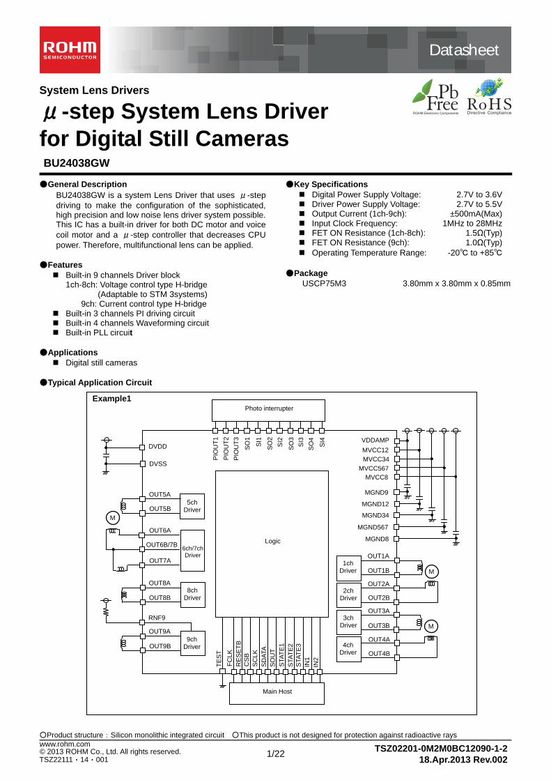
Pin Configuration
J H G F E D C
B A
1 2 3 4 5 6 7 8 9
(Bottom view)
OUT8A OUT6B/7B OUT6A MGND567 OUT7A MVCC567
DVSS
TEST OUT5B OUT5A
MVCC8 OUT8A SCLK FCLK SOUT DVDD DVSS STATE3 PIOUT1
DVSS MGND8 RESETB STATE2 STATE1
DVSS OUT8B PIOUT2 IN2 OUT2B
DVSS MGND9 CSB IN1 MGND12
DVSS OUT9A SDATA SI4 OUT2A
DVSS OUT9B PIOUT3 SO4 MVCC12
VDDAMP RNF9 SI1 SO1 SI2 OUT1A
DVSS
OUT1B SO2 SI3
RNF9 MVCC34 OUT3A OUT3B OUT4A SO3 OUT1A OUT4B MGND34
DatasheetDatasheet
3/22 TSZ02201-0M2M0BC12090-1-2© 2013 ROHM Co., Ltd. All rights reserved.
18.Apr.2013 Rev.002
www.rohm.com
TSZ22111・15・001
BU24038GW
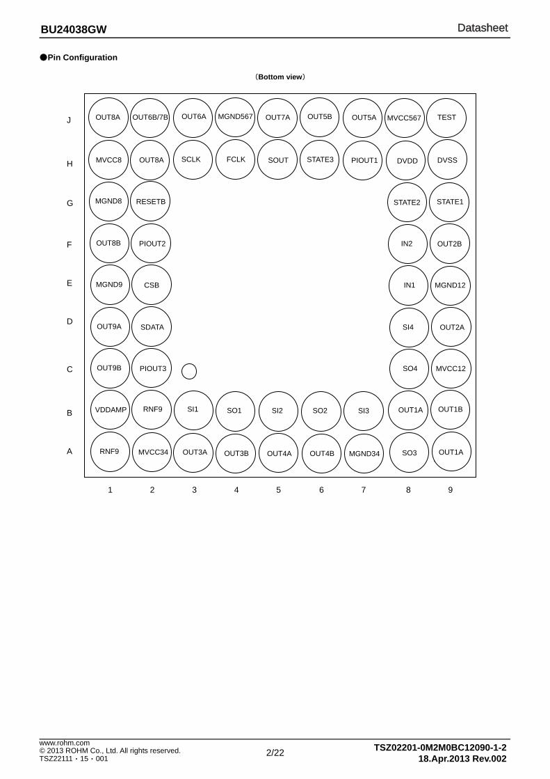
Pin Description Land Matrix
No. Pin Name Power
Supply Function Land Matrix
No. Pin Name Power
Supply Function
H8 DVDD - Digital power supply A9, B8 OUT1A MVCC12 1ch Driver A output
H9 DVSS - ground B9 OUT1B MVCC12 1ch Driver B output
G2 RESETB DVDD RESETB logic input D9 OUT2A MVCC12 2ch Driver A output
H4 FCLK DVDD FCLK logic input F9 OUT2B MVCC12 2ch Driver B output
E2 CSB DVDD CSB logic input A2 MVCC34 - 3ch, 4ch Driver power supply
H3 SCLK DVDD SCLK logic input A7 MGND34 - 3ch, 4ch Driver ground
D2 SDATA DVDD SDATA logic input A3 OUT3A MVCC34 3ch Driver A output
H5 SOUT DVDD SOUT logic output A4 OUT3B MVCC34 3ch Driver B output
E8 IN1 DVDD IN1 logic input A5 OUT4A MVCC34 4ch Driver A output
F8 IN2 DVDD IN2 logic input A6 OUT4B MVCC34 4ch Driver B output
G9 STATE1 DVDD STATE1 logic input/output J8 MVCC567 - 5ch, 6ch, 7ch Driver power supply
G8 STATE2 DVDD STATE2 logic input/output J4 MGND567 - 5ch, 6ch, 7ch Driver ground
H6 STATE3 DVDD STATE3 logic input/output J7 OUT5A MVCC567 5ch Driver A output
J9 TEST DVDD TEST logic input J6 OUT5B MVCC567 5ch Driver B output
H7 PIOUT1 DVDD PI driving output 1 J3 OUT6A MVCC567 6ch Driver A output
F2 PIOUT2 DVDD PI driving output 2 J2 OUT6B/7B MVCC567 6ch, 7ch Driver B output
C2 PIOUT3 DVDD PI driving output 3 J5 OUT7A MVCC567 7ch Driver A output
B3 SI1 DVDD Waveforming input1 H1 MVCC8 - 8ch Driver power supply
B4 SO1 DVDD Waveforming output1 G1 MGND8 - 8ch Driver ground
B5 SI2 DVDD Waveforming input2 H2, J1 OUT8A MVCC8 8ch Driver A output
B6 SO2 DVDD Waveforming output2 F1 OUT8B MVCC8 8ch Driver B output
B7 SI3 DVDD Waveforming input3 B1 VDDAMP - 9ch Power supply of current driver control
A8 SO3 DVDD Waveforming output3 A1, B2 RNF9 - 9ch Driver power supply
D8 SI4 DVDD Waveforming input4 E1 MGND9 - 9ch Driver ground
C8 SO4 DVDD Waveforming output4 D1 OUT9A RNF9 9ch Driver A output
C9 MVCC12 - 1ch, 2ch Driver power supply C1 OUT9B RNF9 9ch Driver B output
E9 MGND12 - 1ch, 2ch Driver ground
DatasheetDatasheet
4/22 TSZ02201-0M2M0BC12090-1-2© 2013 ROHM Co., Ltd. All rights reserved.
18.Apr.2013 Rev.002
www.rohm.com
TSZ22111・15・001
BU24038GW
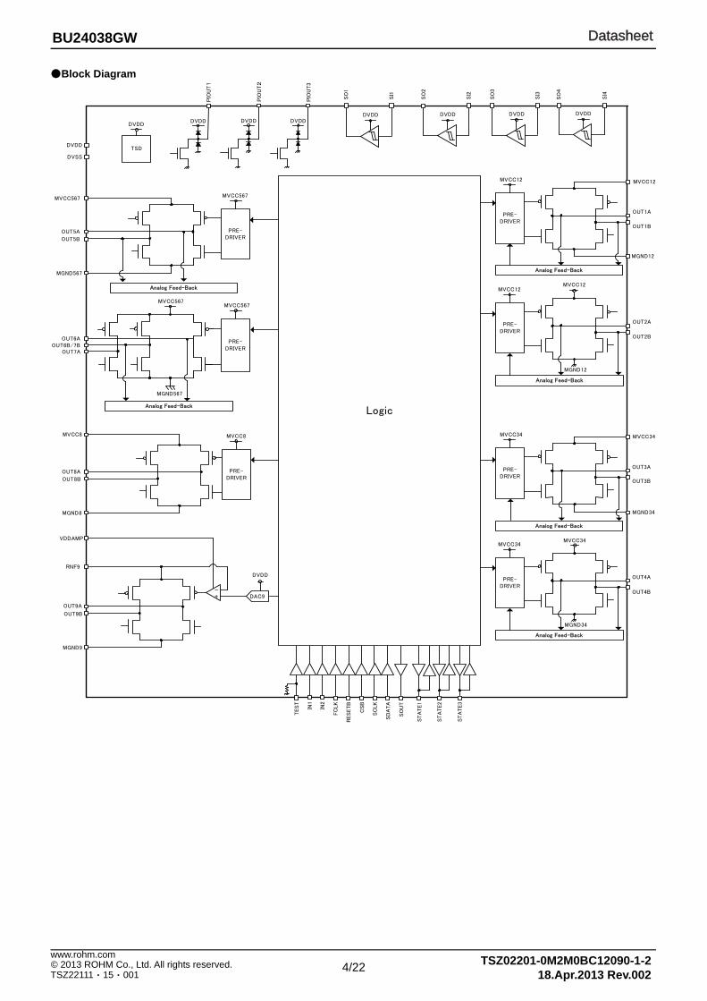
Block Diagram
TSD
DVDD
DVDD
DVSS
OUT8A
OUT8B
SI4
DVDD
PIO
UT3
SO
4
SI3
DVDD
SO
3
SI2
DVDD
SO
2
MVCC8
IN1
IN2
STA
TE1
STA
TE2
STA
TE3
MGND8
OUT5A
OUT5B
OUT6AOUT6B/7B
MVCC567
PRE-DRIVER
MVCC567
PRE-DRIVER
MVCC567
MGND567
MVCC567
MGND567
MVCC8
PRE-DRIVER
SI1
DVDD
SO
1OUT7A
DVDD
PIO
UT2
DVDD
PIO
UT1
DVDD
OUT1A
OUT1B
OUT2A
OUT2B
MVCC12
PRE-DRIVER
MVCC12
PRE-DRIVER
OUT3A
OUT3B
OUT4A
OUT4B
MVCC34
PRE-DRIVER
MVCC34
PRE-DRIVER
MVCC34
MGND34
MVCC12
MGND12
Analog Feed-Back
Analog Feed-Back
Analog Feed-Back
Analog Feed-Back
MVCC12
MGND12
MVCC34
MGND34
Analog Feed-Back
Analog Feed-Back
RNF9
OUT9A
OUT9B
+-
DAC9
DVDD
VDDAMP
MGND9
TEST
Logic
FC
LK
CS
B
SC
LK
SD
ATA
RESETB
SO
UT
DatasheetDatasheet
5/22 TSZ02201-0M2M0BC12090-1-2© 2013 ROHM Co., Ltd. All rights reserved.
18.Apr.2013 Rev.002
www.rohm.com
TSZ22111・15・001
BU24038GW
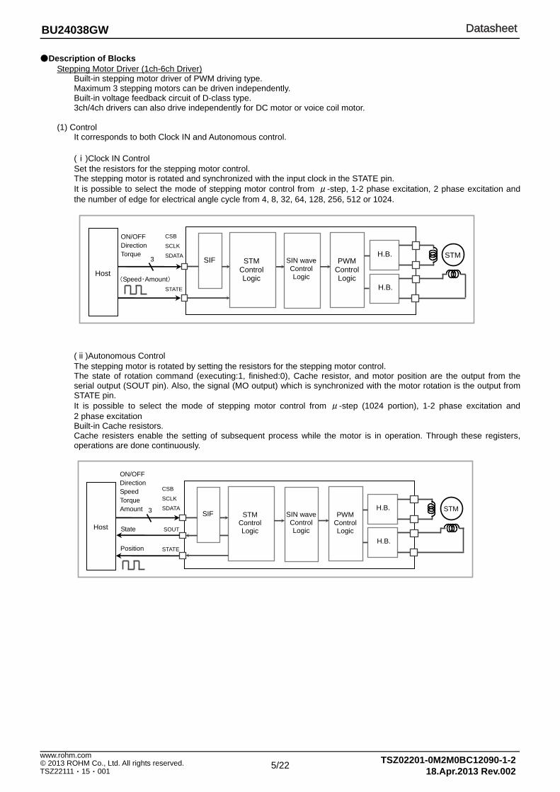
Description of Blocks Stepping Motor Driver (1ch-6ch Driver)
Built-in stepping motor driver of PWM driving type. Maximum 3 stepping motors can be driven independently. Built-in voltage feedback circuit of D-class type. 3ch/4ch drivers can also drive independently for DC motor or voice coil motor.
(1) Control
It corresponds to both Clock IN and Autonomous control.
(ⅰ)Clock IN Control Set the resistors for the stepping motor control. The stepping motor is rotated and synchronized with the input clock in the STATE pin. It is possible to select the mode of stepping motor control from μ-step, 1-2 phase excitation, 2 phase excitation and the number of edge for electrical angle cycle from 4, 8, 32, 64, 128, 256, 512 or 1024.
(ⅱ)Autonomous Control The stepping motor is rotated by setting the resistors for the stepping motor control. The state of rotation command (executing:1, finished:0), Cache resistor, and motor position are the output from the serial output (SOUT pin). Also, the signal (MO output) which is synchronized with the motor rotation is the output from STATE pin. It is possible to select the mode of stepping motor control from μ-step (1024 portion), 1-2 phase excitation and 2 phase excitation Built-in Cache resistors. Cache resisters enable the setting of subsequent process while the motor is in operation. Through these registers, operations are done continuously.
SIN wave Control Logic
PWM ControlLogic
SIF H.B.
H.B.
Host
ON/OFF Direction Torque
(Speed・Amount) STATE
CSB
SCLK
SDATA 3 STM
SIN wave Control Logic
PWM ControlLogic
SIF STM Control Logic
H.B.
H.B.
Host
ON/OFF Direction Speed Torque Amount
State
STATE
CSB
SCLK
SDATA 3 STM
Position
SOUT
STM Control Logic
DatasheetDatasheet
6/22 TSZ02201-0M2M0BC12090-1-2© 2013 ROHM Co., Ltd. All rights reserved.
18.Apr.2013 Rev.002
www.rohm.com
TSZ22111・15・001
BU24038GW
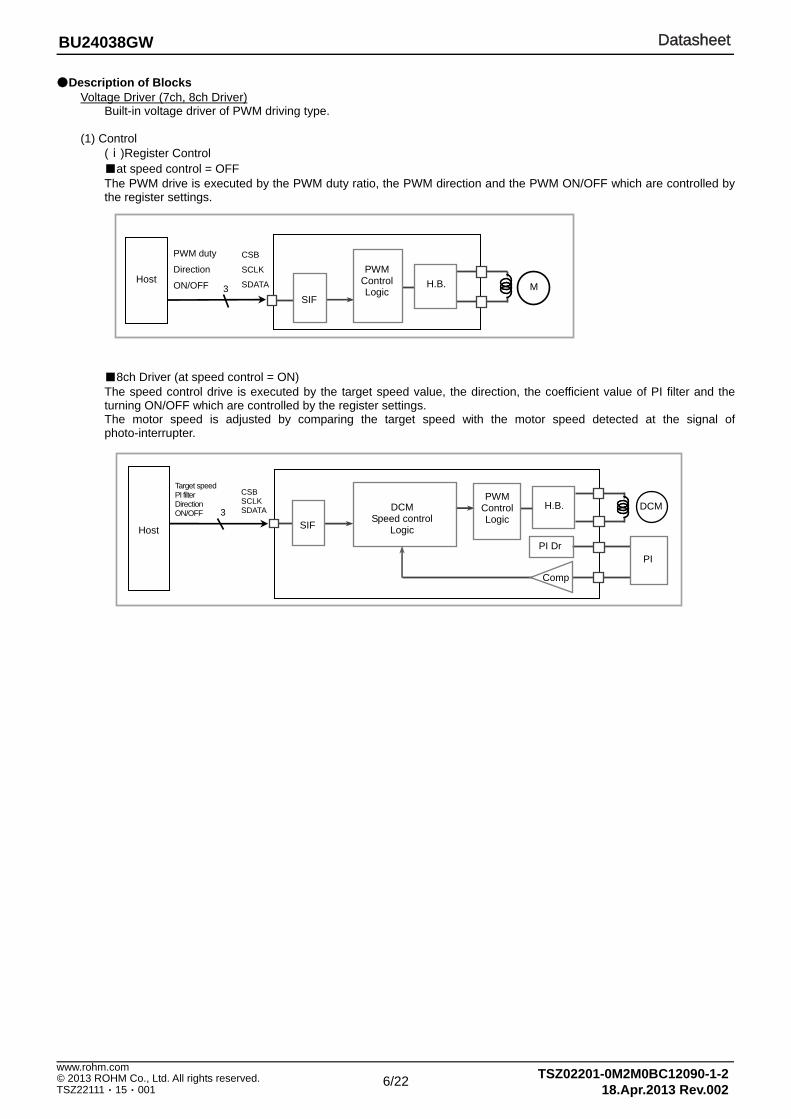
Description of Blocks Voltage Driver (7ch, 8ch Driver)
Built-in voltage driver of PWM driving type.
(1) Control (ⅰ)Register Control at speed control = OFF The PWM drive is executed by the PWM duty ratio, the PWM direction and the PWM ON/OFF which are controlled by the register settings.
8ch Driver (at speed control = ON) The speed control drive is executed by the target speed value, the direction, the coefficient value of PI filter and the turning ON/OFF which are controlled by the register settings. The motor speed is adjusted by comparing the target speed with the motor speed detected at the signal of photo-interrupter.
Host
PWM duty
Direction
ON/OFF
CSB
SCLK
SDATA 3
PWM ControlLogic M
H.B.
Host
Target speed PI filter Direction ON/OFF
CSB SCLK SDATA 3 DCM DCM
Speed control Logic
PI PI Dr
Comp
PWM ControlLogic
SIF H.B.
SIF
DatasheetDatasheet
7/22 TSZ02201-0M2M0BC12090-1-2© 2013 ROHM Co., Ltd. All rights reserved.
18.Apr.2013 Rev.002
www.rohm.com
TSZ22111・15・001
BU24038GW
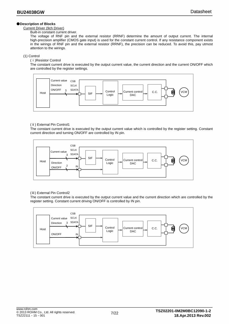
Description of Blocks Current Driver (9ch Driver)
Built-in constant current driver. The voltage of RNF pin and the external resistor (RRNF) determine the amount of output current. The internal high-precision amplifier (CMOS gate input) is used for the constant current control. If any resistance component exists in the wirings of RNF pin and the external resistor (RRNF), the precision can be reduced. To avoid this, pay utmost attention to the wirings.
(1) Control
(ⅰ)Resistor Control The constant current drive is executed by the output current value, the current direction and the current ON/OFF which are controlled by the register settings.
(ⅱ) External Pin Control1 The constant current drive is executed by the output current value which is controlled by the register setting. Constant current direction and turning ON/OFF are controlled by IN pin.
(ⅲ) External Pin Control2 The constant current drive is executed by the output current value and the current direction which are controlled by the register setting. Constant current driving ON/OFF is controlled by IN pin.
Host
Current value
Direction
ON/OFF
CSB
SCLK
SDATA 3 VCM ControlLogic
Current control DAC
C.C.
Current value
CSB
SCLK
SDATA 3
VCM ControlLogic
SIF Current control
DAC C.C. Host
IN Direction
ON/OFF
Current value
Direction
CSB
SCLK
SDATA 3
VCM ControlLogic
Current control DAC
C.C. Host
IN ON/OFF
2
SIF
SIF
DatasheetDatasheet
8/22 TSZ02201-0M2M0BC12090-1-2© 2013 ROHM Co., Ltd. All rights reserved.
18.Apr.2013 Rev.002
www.rohm.com
TSZ22111・15・001
BU24038GW
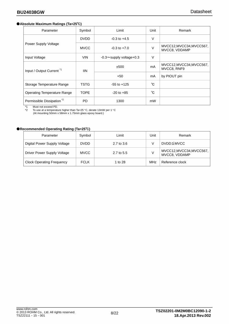
Absolute Maximum Ratings (Ta=25)
Parameter Symbol Limit Unit Remark
DVDD -0.3 to +4.5 V
Power Supply Voltage MVCC -0.3 to +7.0 V MVCC12,MVCC34,MVCC567,
MVCC8, VDDAMP
Input Voltage VIN -0.3~supply voltage+0.3 V
±500 mA MVCC12,MVCC34,MVCC567,MVCC8, RNF9 Input / Output Current *1 IIN
+50 mA by PIOUT pin
Storage Temperature Range TSTG -55 to +125
Operating Temperature Range TOPE -20 to +85
Permissible Dissipation *2 PD 1300 mW
*1 Must not exceed PD. *2 To use at a temperature higher than Ta=25 °C, derate 13mW per 1 °C (At mounting 50mm x 58mm x 1.75mm glass epoxy board.)
Recommended Operating Rating (Ta=25)
Parameter Symbol Limit Unit Remark
Digital Power Supply Voltage DVDD 2.7 to 3.6 V DVDD≦MVCC
Driver Power Supply Voltage MVCC 2.7 to 5.5 V MVCC12,MVCC34,MVCC567,MVCC8, VDDAMP
Clock Operating Frequency FCLK 1 to 28 MHz Reference clock
DatasheetDatasheet
9/22 TSZ02201-0M2M0BC12090-1-2© 2013 ROHM Co., Ltd. All rights reserved.
18.Apr.2013 Rev.002
www.rohm.com
TSZ22111・15・001
BU24038GW
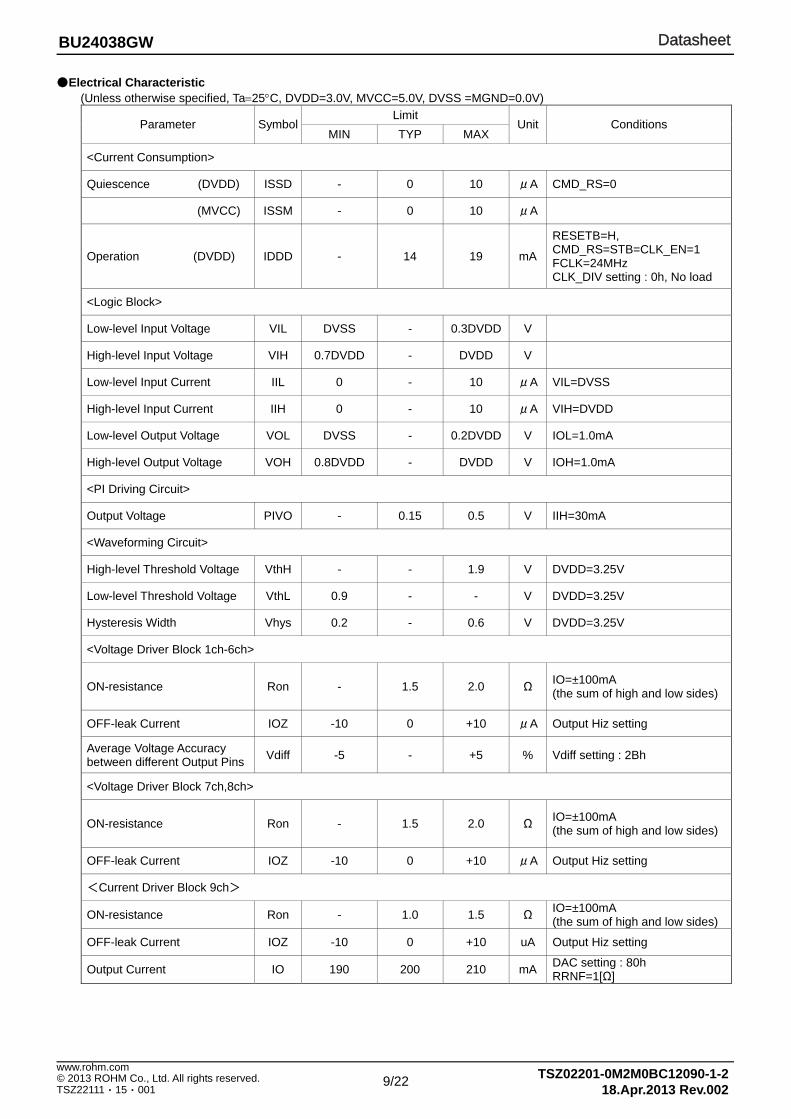
Electrical Characteristic (Unless otherwise specified, Ta=25°C, DVDD=3.0V, MVCC=5.0V, DVSS =MGND=0.0V)
Limit Parameter Symbol
MIN TYP MAX Unit Conditions
<Current Consumption>
Quiescence (DVDD) ISSD - 0 10 μA CMD_RS=0
(MVCC) ISSM - 0 10 μA
Operation (DVDD) IDDD - 14 19 mA
RESETB=H, CMD_RS=STB=CLK_EN=1 FCLK=24MHz CLK_DIV setting : 0h, No load
<Logic Block>
Low-level Input Voltage VIL DVSS - 0.3DVDD V
High-level Input Voltage VIH 0.7DVDD - DVDD V
Low-level Input Current IIL 0 - 10 μA VIL=DVSS
High-level Input Current IIH 0 - 10 μA VIH=DVDD
Low-level Output Voltage VOL DVSS - 0.2DVDD V IOL=1.0mA
High-level Output Voltage VOH 0.8DVDD - DVDD V IOH=1.0mA
<PI Driving Circuit>
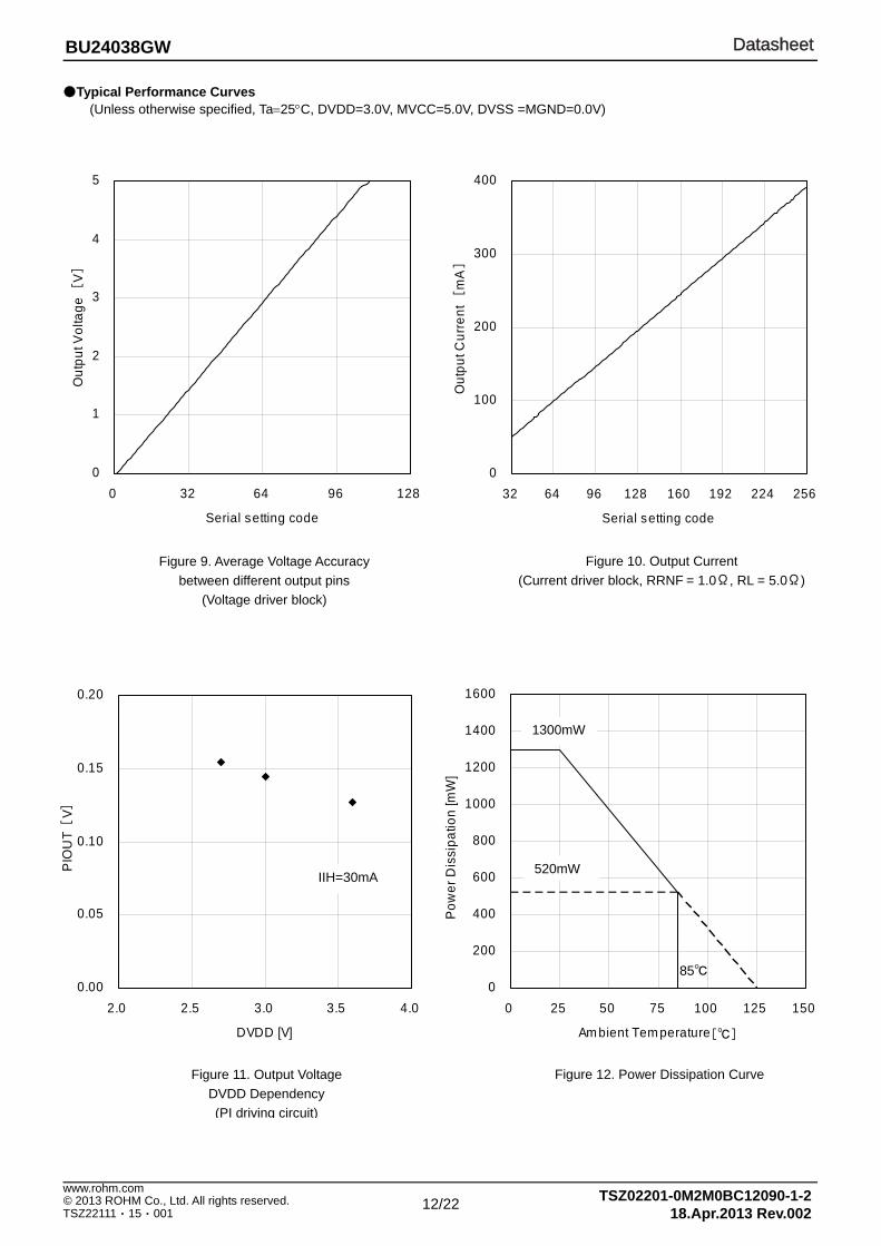
Output Voltage PIVO - 0.15 0.5 V IIH=30mA
<Waveforming Circuit>
High-level Threshold Voltage VthH - - 1.9 V DVDD=3.25V
Low-level Threshold Voltage VthL 0.9 - - V DVDD=3.25V
Hysteresis Width Vhys 0.2 - 0.6 V DVDD=3.25V
<Voltage Driver Block 1ch-6ch>
ON-resistance Ron - 1.5 2.0 Ω IO=±100mA (the sum of high and low sides)
OFF-leak Current IOZ -10 0 +10 μA Output Hiz setting
Average Voltage Accuracy between different Output Pins Vdiff -5 - +5 % Vdiff setting : 2Bh
<Voltage Driver Block 7ch,8ch>
ON-resistance Ron - 1.5 2.0 Ω IO=±100mA (the sum of high and low sides)
OFF-leak Current IOZ -10 0 +10 μA Output Hiz setting
<Current Driver Block 9ch>
ON-resistance Ron - 1.0 1.5 Ω IO=±100mA (the sum of high and low sides)
OFF-leak Current IOZ -10 0 +10 uA Output Hiz setting
Output Current IO 190 200 210 mA DAC setting : 80h RRNF=1[Ω]
DatasheetDatasheet
10/22 TSZ02201-0M2M0BC12090-1-2© 2013 ROHM Co., Ltd. All rights reserved.
18.Apr.2013 Rev.002
www.rohm.com
TSZ22111・15・001
BU24038GW
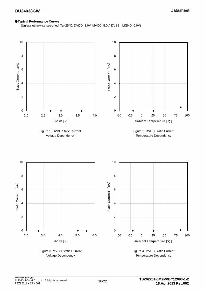
Typical Performance Curves (Unless otherwise specified, Ta=25°C, DVDD=3.0V, MVCC=5.0V, DVSS =MGND=0.0V)
0
2
4
6
8
10
2.0 2.5 3.0 3.5 4.0
DVDD [V]
Stat
ic C
urre
nt
[uA
]
Figure 1. DVDD Static Current Voltage Dependency
0
2
4
6
8
10
2.0 3.0 4.0 5.0 6.0
MVCC [V]
Stat
ic C
urre
nt [
uA]
Figure 3. MVCC Static Current Voltage Dependency
0
2
4
6
8
10
-50 -25 0 25 50 75 100
Am bient Tem perature []
Stat
ic C
urre
nt [
uA]
Figure 2. DVDD Static Current Temperature Dependency
0
2
4
6
8
10
-50 -25 0 25 50 75 100
Am bient Tem perature []
Sta
tic C
urre
ntT
[uA
]
Figure 4. MVCC Static Current Temperature Dependency
DatasheetDatasheet
11/22 TSZ02201-0M2M0BC12090-1-2© 2013 ROHM Co., Ltd. All rights reserved.
18.Apr.2013 Rev.002
www.rohm.com
TSZ22111・15・001
BU24038GW
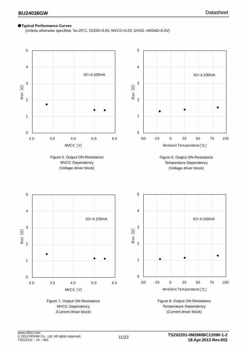
Typical Performance Curves (Unless otherwise specified, Ta=25°C, DVDD=3.0V, MVCC=5.0V, DVSS =MGND=0.0V)
0
1
2
3
4
5
2.0 3.0 4.0 5.0 6.0
MVCC [V]
Ron
[Ω
]
Figure 5. Output ON-Resistance MVCC Dependency (Voltage driver block)
0
1
2
3
4
5
2.0 3.0 4.0 5.0 6.0
MVCC [V]
Ron
[Ω
]
Figure 7. Output ON-Resistance MVCC Dependency (Current driver block)
0
1
2
3
4
5
-50 -25 0 25 50 75 100
Am bient Tem perature[]
Ron
[Ω
]
Figure 6. Output ON-Resistance Temperature Dependency
(Voltage driver block)
0
1
2
3
4
5
-50 -25 0 25 50 75 100
Am bient Tem perature[]
Ron
[Ω
]
Figure 8. Output ON-Resistance Temperature Dependency
(Current driver block)
IO=±100mA
IO=±100mA IO=±100mA
IO=±100mA
DatasheetDatasheet
12/22 TSZ02201-0M2M0BC12090-1-2© 2013 ROHM Co., Ltd. All rights reserved.
18.Apr.2013 Rev.002
www.rohm.com
TSZ22111・15・001
BU24038GW
Typical Performance Curves (Unless otherwise specified, Ta=25°C, DVDD=3.0V, MVCC=5.0V, DVSS =MGND=0.0V)
0
1
2
3
4
5
0 32 64 96 128
Serial setting code
Out
put V
olta
ge [
V]
Figure 9. Average Voltage Accuracy between different output pins
(Voltage driver block)
Figure 10. Output Current (Current driver block, RRNF = 1.0Ω, RL = 5.0Ω)
0.00
0.05
0.10
0.15
0.20
2.0 2.5 3.0 3.5 4.0
DVDD [V]
PIO
UT
[V]
Figure 11. Output Voltage DVDD Dependency (PI driving circuit)
Figure 12. Power Dissipation Curve
0
200
400
600
800
1000
1200
1400
1600
0 25 50 75 100 125 150
Am bient Tem perature[]
Pow
er D
issi
patio
n [m
W]
1300mW
520mW
85
IIH=30mA
0
100
200
300
400
32 64 96 128 160 192 224 256
Serial setting code
Out
put C
urre
nt
[m
A]
DatasheetDatasheet
13/22 TSZ02201-0M2M0BC12090-1-2© 2013 ROHM Co., Ltd. All rights reserved.
18.Apr.2013 Rev.002
www.rohm.com
TSZ22111・15・001
BU24038GW
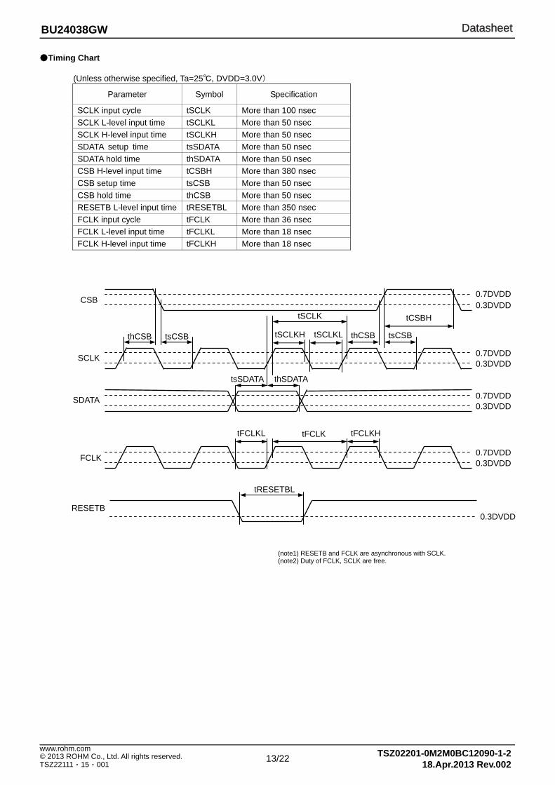
Timing Chart
(Unless otherwise specified, Ta=25, DVDD=3.0V)
Parameter Symbol Specification
SCLK input cycle tSCLK More than 100 nsec SCLK L-level input time tSCLKL More than 50 nsec SCLK H-level input time tSCLKH More than 50 nsec SDATA setup time tsSDATA More than 50 nsec SDATA hold time thSDATA More than 50 nsec CSB H-level input time tCSBH More than 380 nsec CSB setup time tsCSB More than 50 nsec CSB hold time thCSB More than 50 nsec RESETB L-level input time tRESETBL More than 350 nsec FCLK input cycle tFCLK More than 36 nsec FCLK L-level input time tFCLKL More than 18 nsec FCLK H-level input time tFCLKH More than 18 nsec
(note1) RESETB and FCLK are asynchronous with SCLK. (note2) Duty of FCLK, SCLK are free.
CSB
SCLK
SDATA
tCSBH
0.7DVDD0.3DVDD
tsCSB tSCLKL
tSCLK
tSCLKH
0.7DVDD0.3DVDD
thSDATAtsSDATA
0.7DVDD0.3DVDD
tFCLKL tFCLK tFCLKH
FCLK 0.7DVDD0.3DVDD
thCSBthCSB tsCSB
RESETB 0.3DVDD
tRESETBL
DatasheetDatasheet
14/22 TSZ02201-0M2M0BC12090-1-2© 2013 ROHM Co., Ltd. All rights reserved.
18.Apr.2013 Rev.002
www.rohm.com
TSZ22111・15・001
BU24038GW
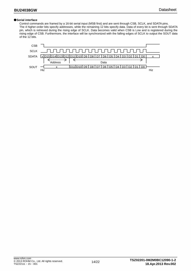
Serial interface Control commands are framed by a 16-bit serial input (MSB first) and are sent through CSB, SCLK, and SDATA pins. The 4 higher-order bits specify addresses, while the remaining 12 bits specify data. Data of every bit is sent through SDATA pin, which is retrieved during the rising edge of SCLK. Data becomes valid when CSB is Low and is registered during the rising edge of CSB. Furthermore, the interface will be synchronized with the falling edges of SCLK to output the SOUT data of the 12 bits.
CSB
D13 D14 D9 D8D10D11 D5 D4D6D7 D1 D0 D2D3 x D15 x D12
Address Data
SCLK
SDATA
D9 D8D10D11 D5 D4D6D7 D1 D0 D2D3xSOUTHiz Hiz
DatasheetDatasheet
15/22 TSZ02201-0M2M0BC12090-1-2© 2013 ROHM Co., Ltd. All rights reserved.
18.Apr.2013 Rev.002
www.rohm.com
TSZ22111・15・001
BU24038GW
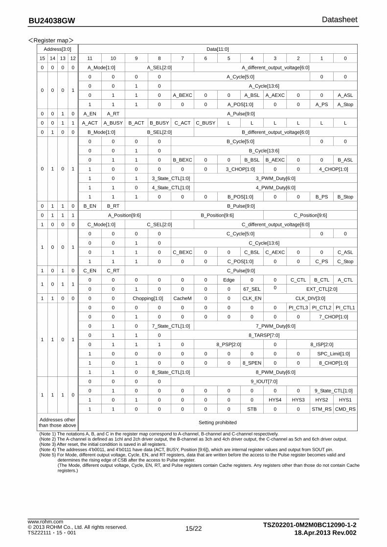
<Register map> Address[3:0] Data[11:0]
15 14 13 12 11 10 9 8 7 6 5 4 3 2 1 0
0 0 0 0 A_Mode[1:0] A_SEL[2:0] A_different_output_voltage[6:0]
0 0 0 0 A_Cycle[5:0] 0 0
0 0 1 0 A_Cycle[13:6]
0 1 1 0 A_BEXC 0 0 A_BSL A_AEXC 0 0 A_ASL0 0 0 1
1 1 1 0 0 0 A_POS[1:0] 0 0 A_PS A_Stop
0 0 1 0 A_EN A_RT A_Pulse[9:0]
0 0 1 1 A_ACT A_BUSY B_ACT B_BUSY C_ACT C_BUSY L L L L L L
0 1 0 0 B_Mode[1:0] B_SEL[2:0] B_different_output_voltage[6:0]
0 0 0 0 B_Cycle[5:0] 0 0
0 0 1 0 B_Cycle[13:6]
0 1 1 0 B_BEXC 0 0 B_BSL B_AEXC 0 0 B_ASL
1 0 0 0 0 0 3_CHOP[1:0] 0 0 4_CHOP[1:0]
1 0 1 3_State_CTL[1:0] 3_PWM_Duty[6:0]
1 1 0 4_State_CTL[1:0] 4_PWM_Duty[6:0]
0 1 0 1
1 1 1 0 0 0 B_POS[1:0] 0 0 B_PS B_Stop
0 1 1 0 B_EN B_RT B_Pulse[9:0]
0 1 1 1 A_Position[9:6] B_Position[9:6] C_Position[9:6]
1 0 0 0 C_Mode[1:0] C_SEL[2:0] C_different_output_voltage[6:0]
0 0 0 0 C_Cycle[5:0] 0 0
0 0 1 0 C_Cycle[13:6]
0 1 1 0 C_BEXC 0 0 C_BSL C_AEXC 0 0 C_ASL1 0 0 1
1 1 1 0 0 0 C_POS[1:0] 0 0 C_PS C_Stop
1 0 1 0 C_EN C_RT C_Pulse[9:0]
0 0 0 0 0 0 Edge 0 0 C_CTL B_CTL A_CTL1 0 1 1
0 0 1 0 0 0 0 67_SEL 0 EXT_CTL[2:0]
1 1 0 0 0 0 Chopping[1:0] CacheM 0 0 CLK_EN CLK_DIV[3:0]
0 0 0 0 0 0 0 0 0 PI_CTL3 PI_CTL2 PI_CTL1
0 0 1 0 0 0 0 0 0 0 7_CHOP[1:0]
0 1 0 7_State_CTL[1:0] 7_PWM_Duty[6:0]
0 1 1 0 8_TARSP[7:0]
0 1 1 1 0 8_PSP[2:0] 0 8_ISP[2:0]
1 0 0 0 0 0 0 0 0 0 SPC_Limit[1:0]
1 0 1 0 0 0 0 8_SPEN 0 0 8_CHOP[1:0]
1 1 0 1
1 1 0 8_State_CTL[1:0] 8_PWM_Duty[6:0]
0 0 0 0 9_IOUT[7:0]
0 1 0 0 0 0 0 0 0 0 9_State_CTL[1:0]
1 0 1 0 0 0 0 0 HYS4 HYS3 HYS2 HYS11 1 1 0
1 1 0 0 0 0 0 STB 0 0 STM_RS CMD_RS
Addresses other than those above Setting prohibited
(Note 1) The notations A, B, and C in the register map correspond to A-channel, B-channel and C-channel respectively. (Note 2) The A-channel is defined as 1chl and 2ch driver output, the B-channel as 3ch and 4ch driver output, the C-channel as 5ch and 6ch driver output. (Note 3) After reset, the initial condition is saved in all registers. (Note 4) The addresses 4’b0011, and 4’b0111 have data (ACT, BUSY, Position [9:6]), which are internal register values and output from SOUT pin. (Note 5) For Mode, different output voltage, Cycle, EN, and RT registers, data that are written before the access to the Pulse register becomes valid and determines the rising edge of CSB after the access to Pulse register.
(The Mode, different output voltage, Cycle, EN, RT, and Pulse registers contain Cache registers. Any registers other than those do not contain Cache registers.)
DatasheetDatasheet
16/22 TSZ02201-0M2M0BC12090-1-2© 2013 ROHM Co., Ltd. All rights reserved.
18.Apr.2013 Rev.002
www.rohm.com
TSZ22111・15・001
BU24038GW
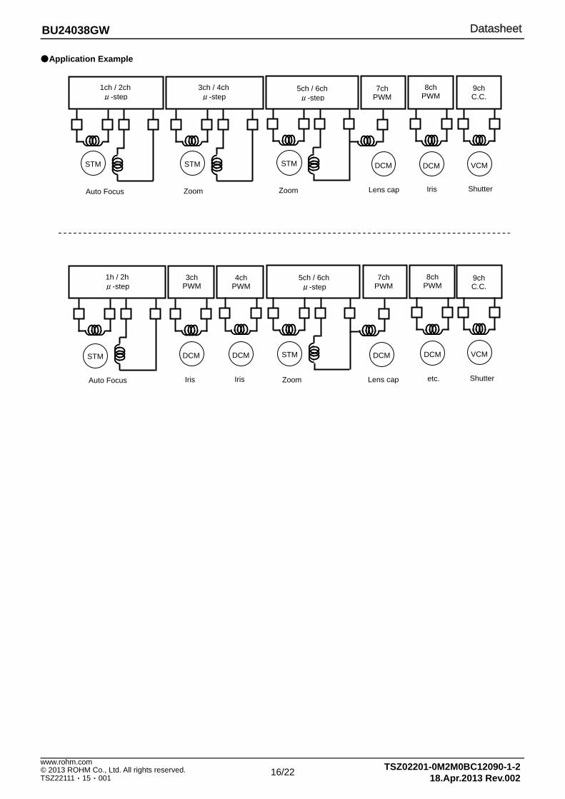
Application Example
STM
Auto Focus
STM
DCM
Iris
VCM
Shutter
1ch / 2ch μ-step
3ch / 4ch μ-step
8ch PWM
9ch C.C.
STM DCM
Zoom Lens cap
5ch / 6ch μ-step
Zoom
7ch PWM
STM
Auto Focus
DCM
Iris
DCM
Iris
1h / 2h μ-step
3ch PWM
4ch PWM
DCM
etc.
VCM
Shutter
8ch PWM
9ch C.C.
STM DCM
Zoom Lens cap
5ch / 6ch μ-step
7ch PWM
DatasheetDatasheet
17/22 TSZ02201-0M2M0BC12090-1-2© 2013 ROHM Co., Ltd. All rights reserved.
18.Apr.2013 Rev.002
www.rohm.com
TSZ22111・15・001
BU24038GW
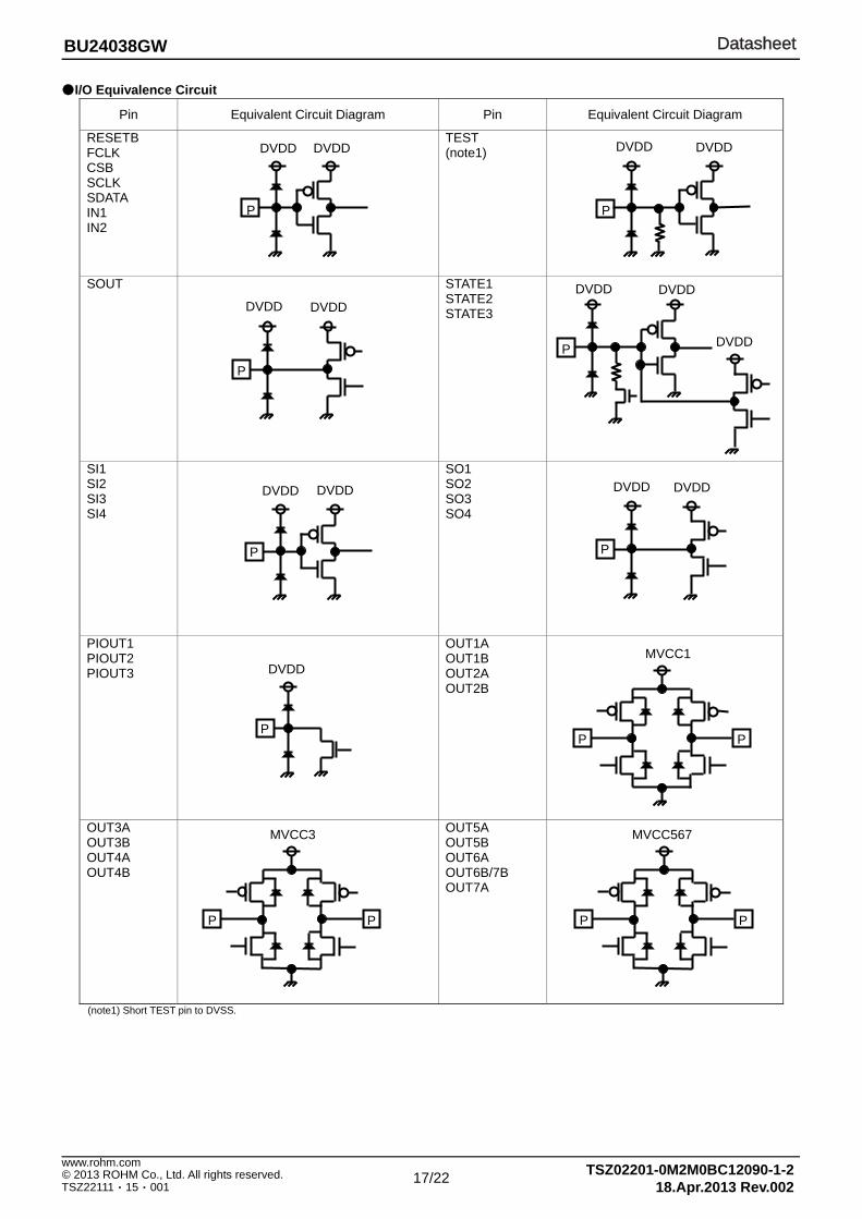
I/O Equivalence Circuit
Pin Equivalent Circuit Diagram Pin Equivalent Circuit Diagram
RESETB FCLK CSB SCLK SDATA IN1 IN2
TEST (note1)
SOUT STATE1 STATE2 STATE3
SI1 SI2 SI3 SI4
SO1 SO2 SO3 SO4
PIOUT1 PIOUT2 PIOUT3
OUT1A OUT1B OUT2A OUT2B
OUT3A OUT3B OUT4A OUT4B
OUT5A OUT5B OUT6A OUT6B/7B OUT7A
(note1) Short TEST pin to DVSS.
P
P P
P P
P
P
P
P P
P
DVDD DVDD DVDD DVDD
DVDD DVDD
DVDD
DVDD DVDD
DVDD MVCC1
MVCC3 MVCC567
PP
DVDD DVDD DVDD DVDD
DatasheetDatasheet
18/22 TSZ02201-0M2M0BC12090-1-2© 2013 ROHM Co., Ltd. All rights reserved.
18.Apr.2013 Rev.002
www.rohm.com
TSZ22111・15・001
BU24038GW
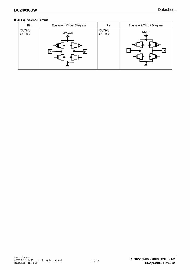
I/O Equivalence Circuit
Pin Equivalent Circuit Diagram Pin Equivalent Circuit Diagram
OUT8A OUT8B
OUT9A OUT9B
P PP P
MVCC8 RNF9

DatasheetDatasheet
19/22 TSZ02201-0M2M0BC12090-1-2© 2013 ROHM Co., Ltd. All rights reserved.
18.Apr.2013 Rev.002
www.rohm.com
TSZ22111・15・001
BU24038GW
Operational Notes 1) Absolute maximum ratings
If applied voltage, operating temperature range, or other absolute maximum ratings are exceeded, the LSI may be damaged. Do not apply voltages or temperatures that exceed the absolute maximum ratings. If you expect that any voltage or temperature could be exceeding the absolute maximum ratings, take physical safety measures such as fuses to prevent any conditions exceeding the absolute maximum ratings from being applied to the LSI.
2) GND potential The voltage of the ground pin must be the lowest voltage of all pins of the IC at all operating conditions. Ensure that no pins are at a voltage below the ground pin at any time, even during transient condition.
3) Thermal design Use a thermal design that allows for a sufficient margin by taking into account the permissible power dissipation (PD) in actual operating conditions.
4) Short circuit between pins and malfunctions Ensure that when mounting the IC on the PCB the direction and position are correct. Incorrect mounting may result in damaging the IC. Avoid nearby pins being shorted to each other especially to ground. Inter-pin shorts could be due to many reasons such as metal particles, water droplets (in very humid environment) and unintentional solder bridge deposited in between pins during assembly to name a few.
5) Operation in strong magnetic field Operating the IC in the presence of a strong electromagnetic field may cause the IC to malfunction.
6) Power ON sequence
To turn ON the DVDD, be sure to reset at RESETB pin. 7) Thermal shutdown
The IC incorporates a built-in thermal shutdown circuit, which is designed to turn off the IC when the internal temperature of the IC reaches a specified value. It is not designed to protect the IC from damage or guarantee its operation. Do not continue to operate the IC after this function is activated. Do not use the IC in conditions where this function will always be activated.
8) PI drive circuit
The output voltage of PIOUT should not exceed the voltage of the power supply voltage DVDD.
DatasheetDatasheet
20/22 TSZ02201-0M2M0BC12090-1-2© 2013 ROHM Co., Ltd. All rights reserved.
18.Apr.2013 Rev.002
www.rohm.com
TSZ22111・15・001
BU24038GW
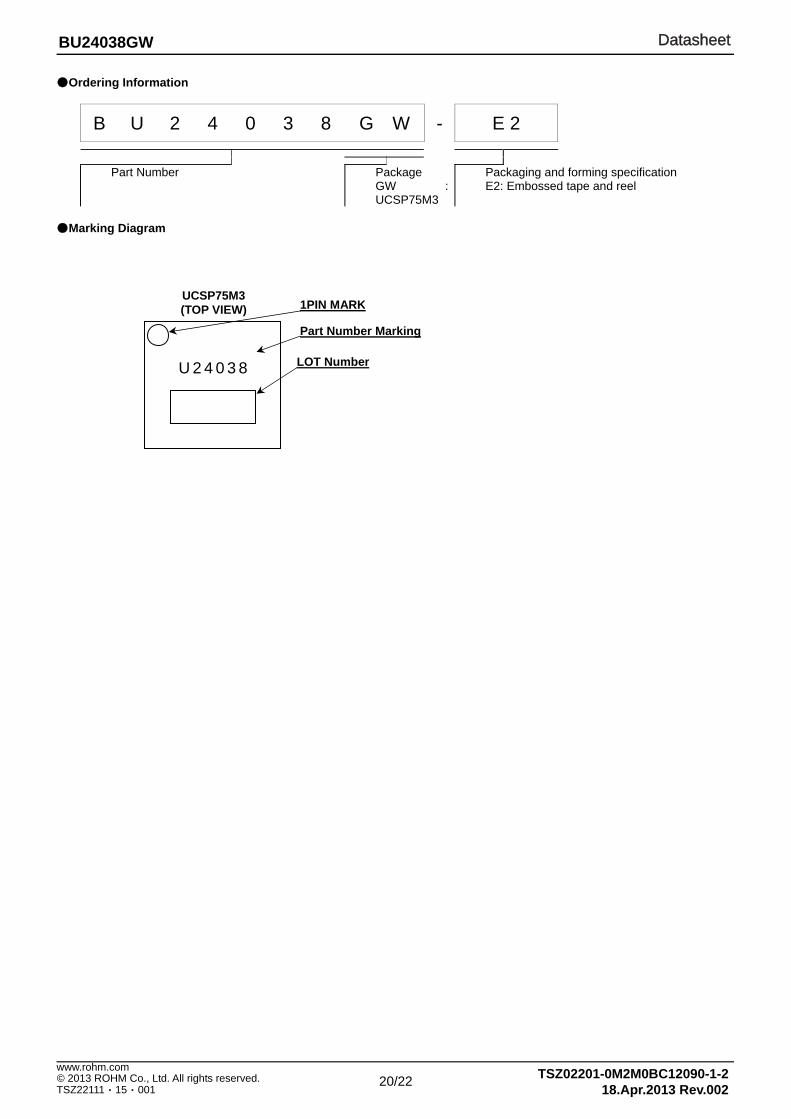
Ordering Information
B U 2 4 0 3 8 G W - E 2
Part Number Package GW : UCSP75M3
Packaging and forming specification E2: Embossed tape and reel
Marking Diagram
UCSP75M3 (TOP VIEW)
U 2 4 0 3 8
Part Number Marking
LOT Number
1PIN MARK
DatasheetDatasheet
21/22 TSZ02201-0M2M0BC12090-1-2© 2013 ROHM Co., Ltd. All rights reserved.
18.Apr.2013 Rev.002
www.rohm.com
TSZ22111・15・001
BU24038GW
Physical Dimension Tape and Reel Information Package Name UCSP75M3
ABC
FGHJ
1 2 3 4 5 6 7 8 9
ED
1PIN MARK
P=0.4×8
S0.8
5MA
X
56-φ0.22±0.05
3.8
0±
0.0
50.3
0±
0.0
5
0.30±0.05
0.1
5±
0.0
7
B
(φ0.15)INDEX POST
S0.06
P=0.4
×8
A
B
0.05 A
3.80±0.05
U24038
Tape Embossed carriertape
Quantity 2,500pcs/Real
Direction of feed
E2(The direction is 1pin product is at the upper leftwhen you hold reel on the hand and you pull outthe tape on the right hand) Reel
Direction of feed1pin
1234 1234 1234 1234 1234 1234
Lot No.

DatasheetDatasheet
22/22 TSZ02201-0M2M0BC12090-1-2© 2013 ROHM Co., Ltd. All rights reserved.
18.Apr.2013 Rev.002
www.rohm.com
TSZ22111・15・001
BU24038GW
Revision History Date Revision Changes
26.Sep.2012 001 New Release 18.Apr.2013 002 Update some English words, sentences, descriptions, grammar and formatting
DatasheetDatasheet
Notice - GE Rev.002© 2014 ROHM Co., Ltd. All rights reserved.
Notice Precaution on using ROHM Products
1. Our Products are designed and manufactured for application in ordinary electronic equipments (such as AV equipment, OA equipment, telecommunication equipment, home electronic appliances, amusement equipment, etc.). If you intend to use our Products in devices requiring extremely high reliability (such as medical equipment (Note 1), transport equipment, traffic equipment, aircraft/spacecraft, nuclear power controllers, fuel controllers, car equipment including car accessories, safety devices, etc.) and whose malfunction or failure may cause loss of human life, bodily injury or serious damage to property (“Specific Applications”), please consult with the ROHM sales representative in advance. Unless otherwise agreed in writing by ROHM in advance, ROHM shall not be in any way responsible or liable for any damages, expenses or losses incurred by you or third parties arising from the use of any ROHM’s Products for Specific Applications.
(Note1) Medical Equipment Classification of the Specific Applications JAPAN USA EU CHINA
CLASSⅢ CLASSⅢ
CLASSⅡb CLASSⅢ
CLASSⅣ CLASSⅢ
2. ROHM designs and manufactures its Products subject to strict quality control system. However, semiconductor
products can fail or malfunction at a certain rate. Please be sure to implement, at your own responsibilities, adequate safety measures including but not limited to fail-safe design against the physical injury, damage to any property, which a failure or malfunction of our Products may cause. The following are examples of safety measures:
[a] Installation of protection circuits or other protective devices to improve system safety [b] Installation of redundant circuits to reduce the impact of single or multiple circuit failure
3. Our Products are designed and manufactured for use under standard conditions and not under any special or extraordinary environments or conditions, as exemplified below. Accordingly, ROHM shall not be in any way responsible or liable for any damages, expenses or losses arising from the use of any ROHM’s Products under any special or extraordinary environments or conditions. If you intend to use our Products under any special or extraordinary environments or conditions (as exemplified below), your independent verification and confirmation of product performance, reliability, etc, prior to use, must be necessary:
[a] Use of our Products in any types of liquid, including water, oils, chemicals, and organic solvents [b] Use of our Products outdoors or in places where the Products are exposed to direct sunlight or dust [c] Use of our Products in places where the Products are exposed to sea wind or corrosive gases, including Cl2,
H2S, NH3, SO2, and NO2
[d] Use of our Products in places where the Products are exposed to static electricity or electromagnetic waves [e] Use of our Products in proximity to heat-producing components, plastic cords, or other flammable items [f] Sealing or coating our Products with resin or other coating materials [g] Use of our Products without cleaning residue of flux (even if you use no-clean type fluxes, cleaning residue of
flux is recommended); or Washing our Products by using water or water-soluble cleaning agents for cleaning residue after soldering
[h] Use of the Products in places subject to dew condensation
4. The Products are not subject to radiation-proof design. 5. Please verify and confirm characteristics of the final or mounted products in using the Products. 6. In particular, if a transient load (a large amount of load applied in a short period of time, such as pulse. is applied,
confirmation of performance characteristics after on-board mounting is strongly recommended. Avoid applying power exceeding normal rated power; exceeding the power rating under steady-state loading condition may negatively affect product performance and reliability.
7. De-rate Power Dissipation (Pd) depending on Ambient temperature (Ta). When used in sealed area, confirm the actual
ambient temperature. 8. Confirm that operation temperature is within the specified range described in the product specification. 9. ROHM shall not be in any way responsible or liable for failure induced under deviant condition from what is defined in
this document.
Precaution for Mounting / Circuit board design 1. When a highly active halogenous (chlorine, bromine, etc.) flux is used, the residue of flux may negatively affect product
performance and reliability. 2. In principle, the reflow soldering method must be used; if flow soldering method is preferred, please consult with the
ROHM representative in advance. For details, please refer to ROHM Mounting specification

DatasheetDatasheet
Notice - GE Rev.002© 2014 ROHM Co., Ltd. All rights reserved.
Precautions Regarding Application Examples and External Circuits 1. If change is made to the constant of an external circuit, please allow a sufficient margin considering variations of the
characteristics of the Products and external components, including transient characteristics, as well as static characteristics.
2. You agree that application notes, reference designs, and associated data and information contained in this document
are presented only as guidance for Products use. Therefore, in case you use such information, you are solely responsible for it and you must exercise your own independent verification and judgment in the use of such information contained in this document. ROHM shall not be in any way responsible or liable for any damages, expenses or losses incurred by you or third parties arising from the use of such information.
Precaution for Electrostatic
This Product is electrostatic sensitive product, which may be damaged due to electrostatic discharge. Please take proper caution in your manufacturing process and storage so that voltage exceeding the Products maximum rating will not be applied to Products. Please take special care under dry condition (e.g. Grounding of human body / equipment / solder iron, isolation from charged objects, setting of Ionizer, friction prevention and temperature / humidity control).
Precaution for Storage / Transportation 1. Product performance and soldered connections may deteriorate if the Products are stored in the places where:
[a] the Products are exposed to sea winds or corrosive gases, including Cl2, H2S, NH3, SO2, and NO2 [b] the temperature or humidity exceeds those recommended by ROHM [c] the Products are exposed to direct sunshine or condensation [d] the Products are exposed to high Electrostatic
2. Even under ROHM recommended storage condition, solderability of products out of recommended storage time period may be degraded. It is strongly recommended to confirm solderability before using Products of which storage time is exceeding the recommended storage time period.
3. Store / transport cartons in the correct direction, which is indicated on a carton with a symbol. Otherwise bent leads
may occur due to excessive stress applied when dropping of a carton. 4. Use Products within the specified time after opening a humidity barrier bag. Baking is required before using Products of
which storage time is exceeding the recommended storage time period.
Precaution for Product Label QR code printed on ROHM Products label is for ROHM’s internal use only.
Precaution for Disposition When disposing Products please dispose them properly using an authorized industry waste company.
Precaution for Foreign Exchange and Foreign Trade act Since our Products might fall under controlled goods prescribed by the applicable foreign exchange and foreign trade act, please consult with ROHM representative in case of export.
Precaution Regarding Intellectual Property Rights 1. All information and data including but not limited to application example contained in this document is for reference
only. ROHM does not warrant that foregoing information or data will not infringe any intellectual property rights or any other rights of any third party regarding such information or data. ROHM shall not be in any way responsible or liable for infringement of any intellectual property rights or other damages arising from use of such information or data.:
2. No license, expressly or implied, is granted hereby under any intellectual property rights or other rights of ROHM or any
third parties with respect to the information contained in this document.
Other Precaution 1. This document may not be reprinted or reproduced, in whole or in part, without prior written consent of ROHM. 2. The Products may not be disassembled, converted, modified, reproduced or otherwise changed without prior written
consent of ROHM. 3. In no event shall you use in any way whatsoever the Products and the related technical information contained in the
Products or this document for any military purposes, including but not limited to, the development of mass-destruction weapons.
4. The proper names of companies or products described in this document are trademarks or registered trademarks of
ROHM, its affiliated companies or third parties.

DatasheetDatasheet
Notice – WE Rev.001© 2014 ROHM Co., Ltd. All rights reserved.
General Precaution 1. Before you use our Pro ducts, you are requested to care fully read this document and fully understand its contents.
ROHM shall n ot be in an y way responsible or liabl e for fa ilure, malfunction or acci dent arising from the use of a ny ROHM’s Products against warning, caution or note contained in this document.
2. All information contained in this docume nt is current as of the issuing date and subj ect to change without any prior
notice. Before purchasing or using ROHM’s Products, please confirm the la test information with a ROHM sale s representative.
3. The information contained in this doc ument is provi ded on an “as is” basis and ROHM does not warrant that all
information contained in this document is accurate an d/or error-free. ROHM shall not be in an y way responsible or liable for any damages, expenses or losses incurred by you or third parties resulting from inaccuracy or errors of or concerning such information.