μ-SLS of Metals: Physical and thermal characterization of ...
17
μ-SLS of Metals: Physical and thermal characterization of Cu- nanopowders N.K. Roy*, A. Yuksel* and M.A. Cullinan* *Department of Mechanical Engineering, The University of Texas at Austin, TX 78712 Abstract Micro-scale selective laser sintering(μ-SLS) requires the use of nanoparticles(NPs) since the particle size needs to be an order of magnitude smaller than the melt pool in order to accurately sinter particles together to form a part. Most NPs properties are dependent upon size and thus, an exhaustive study of the physical and thermal properties of these NPs is required in order to successfully model and simulate the sintering process. In this paper we will present particle size characterization using Scanning electron microscopy (SEM), density measurements using He pycnometry, and X-ray Energy Dispersive Spectroscopy that were carried out to characterize the copper(Cu) nanopowder samples. Furthermore, the samples were sintered with different powers to estimate optimum power and exposure times and the results have been discussed along with further scope of work for fully characterizing the particles. Introduction Laser sintering is an additive manufacturing technology that employs a high power laser to fuse the metal powder into a mass that has a desired 3-dimensional shape. The laser selectively scans and fuses powder material on the surface of the powder bed based on the previously generated CAD file. After one layer is scanned, the powder bed is lowered by one layer thickness, creating a new layer that is scanned. The process is repeated until the part is completed [1]. It is important to note the difference between Selective Laser Melting(SLM) and Selective Laser Sintering(SLS). In SLM, the particles are melted and fused together whereas in SLS, the particles are not fully melted . They are heated to a point where the particles can fuse together. The point may be significantly lower than the melting point and can vary depending upon the time of exposure to heat. And hence, the energy requirements per unit mass are lower for SLS as compared to SLM. The smallest feature sizes that the commercially available sintering machines can achieve is of the order of hundreds of microns and this research is focused towards designing a system to achieve 1μm feature sizes [2]. To get that feature size, it is required to use particles smaller than the feature size and hence, NPs were the first choice for the sintering. However, NPs have their own limitations including excessive agglomeration and oxidation. Because of high surface area to volume ratio, the powders have very high surface energy and hence the particles tend to agglomerate to reduce their surface energy. And, van der Waals forces become dominant over gravity at nano-scale. It is because of these reasons that the properties of NPs are significantly different from the bulk properties of the sample. Thus, it is required to carry out a thorough analysis of the physical, thermal properties and optical properties of these NPs in order to develop a model for heat transfer during sintering and to estimate the power requirements for 772
Transcript of μ-SLS of Metals: Physical and thermal characterization of ...
μ-SLS of Metals: Physical and thermal characterization of Cu- nanopowders
N.K. Roy*, A. Yuksel* and M.A. Cullinan* *Department of Mechanical Engineering, The University of Texas at Austin, TX 78712
Abstract
Micro-scale selective laser sintering(μ-SLS) requires the use of nanoparticles(NPs) since the particle size needs to be an order of magnitude smaller than the melt pool in order to accurately sinter particles together to form a part. Most NPs properties are dependent upon size and thus, an exhaustive study of the physical and thermal properties of these NPs is required in order to successfully model and simulate the sintering process. In this paper we will present particle size characterization using Scanning electron microscopy (SEM), density measurements using He pycnometry, and X-ray Energy Dispersive Spectroscopy that were carried out to characterize the copper(Cu) nanopowder samples. Furthermore, the samples were sintered with different powers to estimate optimum power and exposure times and the results have been discussed along with further scope of work for fully characterizing the particles.
Introduction
Laser sintering is an additive manufacturing technology that employs a high power laser to fuse the metal powder into a mass that has a desired 3-dimensional shape. The laser selectively scans and fuses powder material on the surface of the powder bed based on the previously generated CAD file. After one layer is scanned, the powder bed is lowered by one layer thickness, creating a new layer that is scanned. The process is repeated until the part is completed [1]. It is important to note the difference between Selective Laser Melting(SLM) and Selective Laser Sintering(SLS). In SLM, the particles are melted and fused together whereas in SLS, the particles are not fully melted . They are heated to a point where the particles can fuse together. The point may be significantly lower than the melting point and can vary depending upon the time of exposure to heat. And hence, the energy requirements per unit mass are lower for SLS as compared to SLM.
The smallest feature sizes that the commercially available sintering machines can achieve is of the order of hundreds of microns and this research is focused towards designing a system to achieve 1μm feature sizes [2]. To get that feature size, it is required to use particles smaller than the feature size and hence, NPs were the first choice for the sintering. However, NPs have their own limitations including excessive agglomeration and oxidation. Because of high surface area to volume ratio, the powders have very high surface energy and hence the particles tend to agglomerate to reduce their surface energy. And, van der Waals forces become dominant over gravity at nano-scale. It is because of these reasons that the properties of NPs are significantly different from the bulk properties of the sample. Thus, it is required to carry out a thorough analysis of the physical, thermal properties and optical properties of these NPs in order to develop a model for heat transfer during sintering and to estimate the power requirements for
772

sintering depending upon the spot size and layer thickness. A simplified model for power estimation has been presented below.
Pulse energy to sinter a spot size of diameter D and layer thickness, h in n pulses,
En= ρ*π*D2*h*[CP*(Tf-Ti)+lf]/(4*n*(1-R)) (1)
and, Average power, Pavn= En* f (2)
where f= repetition rate of the laser, ρ= density of the powders, CP= Specific heat capacity of the powders, lf= heat of fusion of the powders, Ti= initial temperature of the powder bed, Tf= sintering temperature of the powder bed and R= reflectivity of the powders. This model presents an upper limit estimate of the sintering powers required as it takes into account the melting of the particles while sintering process doesn't involve any melting. Properties like density, absorptivity, specific heat capacity etc. are critical to estimate the powers accurately and thus, the need for the analysis. The primary application for the project is microelectronics packaging and hence, Cu has been chosen because of its good electrical conductivity and low cost as compared to silver and gold.
A. SEM characterization of the particles
Table 1 . Different Powder Samples with their production techniques
For a first hand physical characterization of the particles, Scanning Electron Microscopy(SEM) is a good method to gauge the particle size and their morphology. For the particles greater than 20nm in size, it can provide details about both the individual particle size and also about the extent of agglomeration in the sample.The SEM images of the nanoparticles were taken using FEI Quanta 650 SEM/ESEM.
The samples were prepared by spreading a very thin layer of powders on the carbon tape coated SEM stub. The images were taken using Secondary Electron Detector under the following
S.No Sample Average Particle Size (nm)
Production Method
1 Cu NPs (99.9% purity) from US Research Nano(USRN), Inc 40 Electric Explosion
of Wire (EEW)
2 Cu NPs (99.9% purity) from USRN, Inc 100 Electric Explosion
of Wire
3 Carbon Coated Copper-USRN,Inc 25 Laser Ablation
Synthesis
4 Passivated Copper-USRN,Inc 25 Laser Ablation Synthesis
5 MK Impex -Passivated (99.8% purity) 25 Chemical
reduction
773

conditions unless stated otherwise: High Vacuum( Chamber pressure- 1.13E-5 torr), High Voltage- 20KV and Emission Current- 384μA.
Figure1. a), b), c) and d). SEM micrographs of Cu NPs from USRN with APS 40nm
774
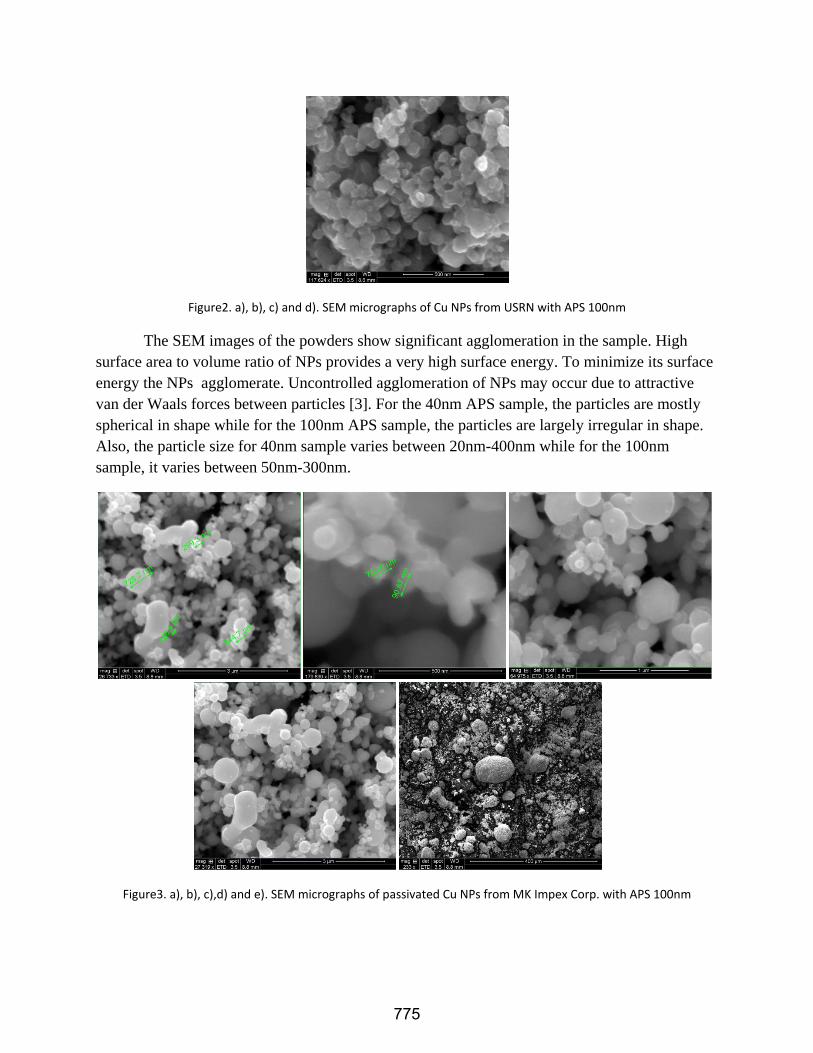
Figure2. a), b), c) and d). SEM micrographs of Cu NPs from USRN with APS 100nm
The SEM images of the powders show significant agglomeration in the sample. High surface area to volume ratio of NPs provides a very high surface energy. To minimize its surface energy the NPs agglomerate. Uncontrolled agglomeration of NPs may occur due to attractive van der Waals forces between particles [3]. For the 40nm APS sample, the particles are mostly spherical in shape while for the 100nm APS sample, the particles are largely irregular in shape. Also, the particle size for 40nm sample varies between 20nm-400nm while for the 100nm sample, it varies between 50nm-300nm.
Figure3. a), b), c),d) and e). SEM micrographs of passivated Cu NPs from MK Impex Corp. with APS 100nm
775
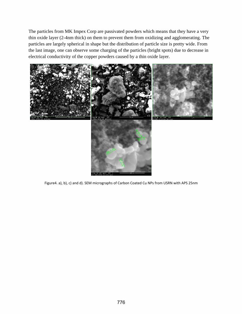
The particles from MK Impex Corp are passivated powders which means that they have a very thin oxide layer (2-4nm thick) on them to prevent them from oxidizing and agglomerating. The particles are largely spherical in shape but the distribution of particle size is pretty wide. From the last image, one can observe some charging of the particles (bright spots) due to decrease in electrical conductivity of the copper powders caused by a thin oxide layer.
Figure4. a), b), c) and d). SEM micrographs of Carbon Coated Cu NPs from USRN with APS 25nm
776

Figure5. a), b), c), d) and e). SEM micrographs of Passivated Cu NPs from USRN with APS 25nm
In both the carbon coated and passivated Cu NPs from USRN, Inc, a lot of edge effect and charging up of the particles was observed which made it difficult to get high resolution images for these particles. Table 1 gives a summary of the results of SEM.
After the SEM characterization, based on particle size range and morphology of the particles, it was decided to go ahead with the 40nm sample from USRN, Inc (prepared by Electric Explosion of Wire) as the particles in the sample have narrow distribution as compared to other samples and are also spherical in shape which affects the heat transfer properties of these particles [4].
B. Skeletal Density measurement
A Quantachrome INSTRUMENT® ULTRAPYC 1200e helium pycnometer was used to measure the skeletal or true density of the copper nanopowder samples[1]. Helium was chosen as a probe gas in that it features a very small atomic size and can permeate the narrow pores in a solid, permitting the determination of the real volume occupied by the sample [5]. Also, it is non-reactive and closely resembles an ideal gas. The mass was measured by a Denver INSTRUMENT® weightometer APX-200.
777
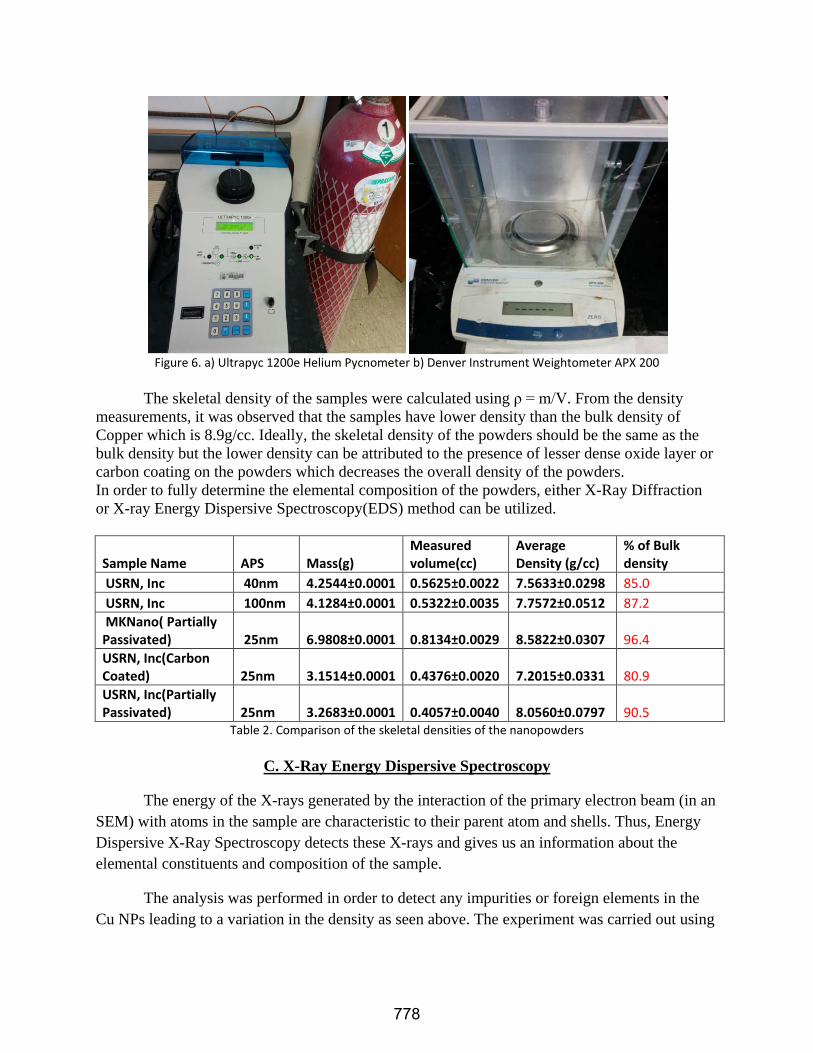
Figure 6. a) Ultrapyc 1200e Helium Pycnometer b) Denver Instrument Weightometer APX 200
The skeletal density of the samples were calculated using ρ = m/V. From the density measurements, it was observed that the samples have lower density than the bulk density of Copper which is 8.9g/cc. Ideally, the skeletal density of the powders should be the same as the bulk density but the lower density can be attributed to the presence of lesser dense oxide layer or carbon coating on the powders which decreases the overall density of the powders. In order to fully determine the elemental composition of the powders, either X-Ray Diffraction or X-ray Energy Dispersive Spectroscopy(EDS) method can be utilized.
Sample Name APS Mass(g) Measured volume(cc)
Average Density (g/cc)
% of Bulk density
USRN, Inc 40nm 4.2544±0.0001 0.5625±0.0022 7.5633±0.0298 85.0 USRN, Inc 100nm 4.1284±0.0001 0.5322±0.0035 7.7572±0.0512 87.2 MKNano( Partially Passivated) 25nm 6.9808±0.0001 0.8134±0.0029 8.5822±0.0307 96.4 USRN, Inc(Carbon Coated) 25nm 3.1514±0.0001 0.4376±0.0020 7.2015±0.0331 80.9 USRN, Inc(Partially Passivated) 25nm 3.2683±0.0001 0.4057±0.0040 8.0560±0.0797 90.5
Table 2. Comparison of the skeletal densities of the nanopowders
C. X-Ray Energy Dispersive Spectroscopy
The energy of the X-rays generated by the interaction of the primary electron beam (in an SEM) with atoms in the sample are characteristic to their parent atom and shells. Thus, Energy Dispersive X-Ray Spectroscopy detects these X-rays and gives us an information about the elemental constituents and composition of the sample.
The analysis was performed in order to detect any impurities or foreign elements in the Cu NPs leading to a variation in the density as seen above. The experiment was carried out using
778

FEI Quanta 650 SEM/ESEM under the same operating conditions as stated in the SEM characterization section and the images for different samples are attached below:
Figure 7. USRN,Inc -40nm.In this figure, the peaks correspond to Kα(8.04kev), Lα(0.93kev) and Kβ(8.93kev) of Copper, Kα(0.525kev) of oxygen and Kα (0.277kev) of Carbon. Oxygen peak suggests that the particles are definitely
oxidised and carbon peak is probably due to the carbon tape on the SEM stub
Figure 8 a) and b) . USRN, Inc-100nm- In this sample, an unusual peak Kα (0.677kev) of iron which suggests that there is some trace quantity of iron in the sample as well was noted
779
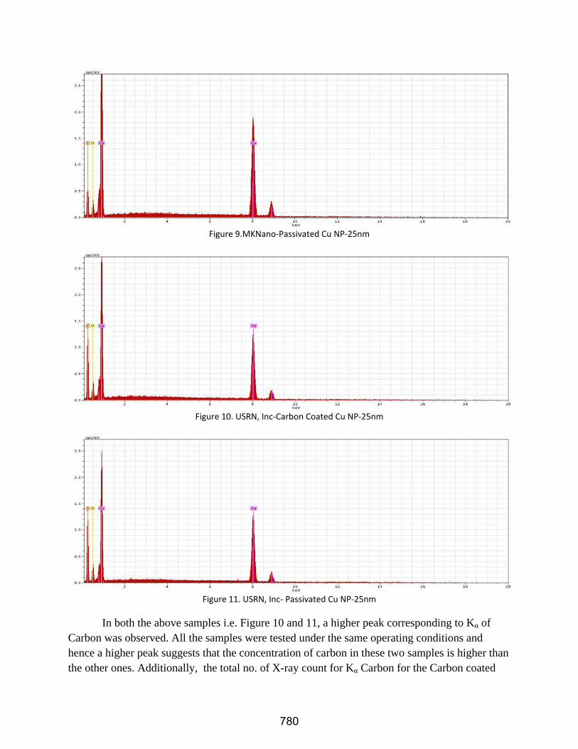
Figure 9.MKNano-Passivated Cu NP-25nm
Figure 10. USRN, Inc-Carbon Coated Cu NP-25nm
Figure 11. USRN, Inc- Passivated Cu NP-25nm
In both the above samples i.e. Figure 10 and 11, a higher peak corresponding to Kα of Carbon was observed. All the samples were tested under the same operating conditions and hence a higher peak suggests that the concentration of carbon in these two samples is higher than the other ones. Additionally, the total no. of X-ray count for Kα Carbon for the Carbon coated
780

and passivated Copper powder sample from US Research Nanomaterials, is 3 times as compared to the X-ray count of Kα Carbon for the other samples which ascertains the possibility of a higher carbon content in those two powder samples.
Full scale count
Cu O C Fe Sample Name APS
USRN, Inc 40nm 16800 200 100 USRN, Inc 100nm 16700 300 100 100 MKNano( Partially Passivated) 25nm 19900 200 100 USRN, Inc(Carbon Coated) 25nm 15900 200 300 USRN, Inc(Partially Passivated) 25nm 15200 200 300
Table 3. Full scale count of the X-rays corresponding to each element in different samples
From the EDS analysis, it is observed that the 40nm sample from USRN, Inc (by EEW method) has lower impurities ( in terms of extent of Carbon and traces of Iron) compared to the other samples and hence, the choice for further sintering experiments.
D. Sintering Experiments
Figure 19 shows the femto-second laser sintering setup. A Q-switched Ti-Sapphire Laser(Spitfire Ace from Spectra Physics)) using a light of wavelength 800nm at a repetition rate of 5KHz and a pulse width of around 100fs was used as the laser source. A mechanical shutter for controlling the number of pulses hitting the sample was operated with a maximum frequency of 1 KHz. The laser beam was fixed and focused using an infinity corrected long range objective lens (Mitutoyo 10X and NA 0.23). A beam splitter and polarizer were used for controlling the intensity of the laser beam. In addition, a CCD camera and a white light source were also installed to monitor the system while doing the experiments and it also aided in focusing the objective lens and determination of the spot size. The purpose of these experiments was to validate the power estimation model and observe how the morphology of the powders changes when exposed to different powers for different exposure times.
781
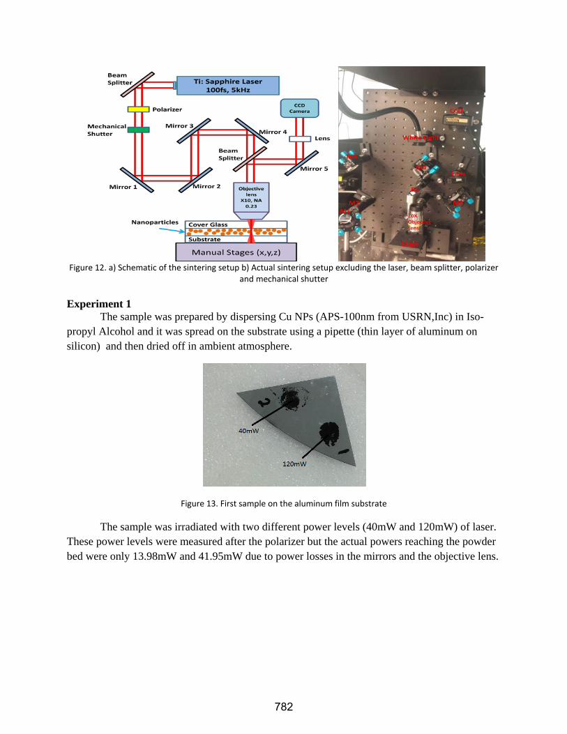
Figure 12. a) Schematic of the sintering setup b) Actual sintering setup excluding the laser, beam splitter, polarizer
and mechanical shutter Experiment 1 The sample was prepared by dispersing Cu NPs (APS-100nm from USRN,Inc) in Iso-propyl Alcohol and it was spread on the substrate using a pipette (thin layer of aluminum on silicon) and then dried off in ambient atmosphere.
Figure 13. First sample on the aluminum film substrate
The sample was irradiated with two different power levels (40mW and 120mW) of laser. These power levels were measured after the polarizer but the actual powers reaching the powder bed were only 13.98mW and 41.95mW due to power losses in the mirrors and the objective lens.
782

Figure 14. a) and b) SEM micrographs of the lines sintered with 40mW of power for 20s under different magnifications
A line created with 40mW of power (20s exposure time) and seen under an SEM (features of SEM). The displacement of powders and damage to the substrate could be attributed to the high power of the source.
Figure 15. a) SEM micrographs of the line sintered with 120mW of power for 20s.b) SEM image showing charging up of the particles
A line created with 120mW of power and 20s exposure time. It clearly suggests that these powers and exposure times are considerably too high to do any sintering. Infact, with these power levels and such high exposure times, the powders were being blown away by the laser. While taking the SEM images, the charging effect of the particles was prominent and it wasn't encountered in any of the previous SEM of the samples suggesting that these particles were not very electrically conductive. This could be due to organic residue being left on the particles once
783

the alcohol was dried off, resulting in lower conductivity of the sample. To get better quality images, the accelerating voltage was reduced and operated under low pressure of water vapor. Experiment 2 First, some power estimation calculations were performed to get a rough estimate of power levels and exposure times that should be used for optimum sintering. Following table gives an estimate of the power required to sinter a spot size of 10 micron and a layer thickness of 1 micron. The calculations take into account melting of powders and hence give an upper estimate of the power requirements.
Estimated Power Required for melting a spot size of diameter 10 micron (mW)(this takes into account the losses due to objective lens)
Exposure Time (ms) Thickness of the layer(microns)
1 5 10 100 500
1 0.721 3.605 7.209 72.090 360.450 5 0.145 0.724 1.448 14.480 72.400 10 0.072 0.361 0.721 7.210 36.050 20 0.036 0.180 0.360 3.600 18.000 25 0.029 0.144 0.288 2.880 14.400
Table 4. Power estimates for different layer thicknesses and different exposure times taking into account the losses of the objective lens
The power retention factor for the objective lens being used was 0.34956.
The sample was prepared by mixing 0.1718g of Cu NPs from USRN, Inc in 5ml of distilled water and then the vial was agitated manually. Few drops of the sample were transferred to the aluminum coated substrate and the wafer was heated at 80 degrees C for 15 minutes using a hot plate (Corning PC-620D)
Figure 16. a) Sample being heated at 80 degrees Celsius
784
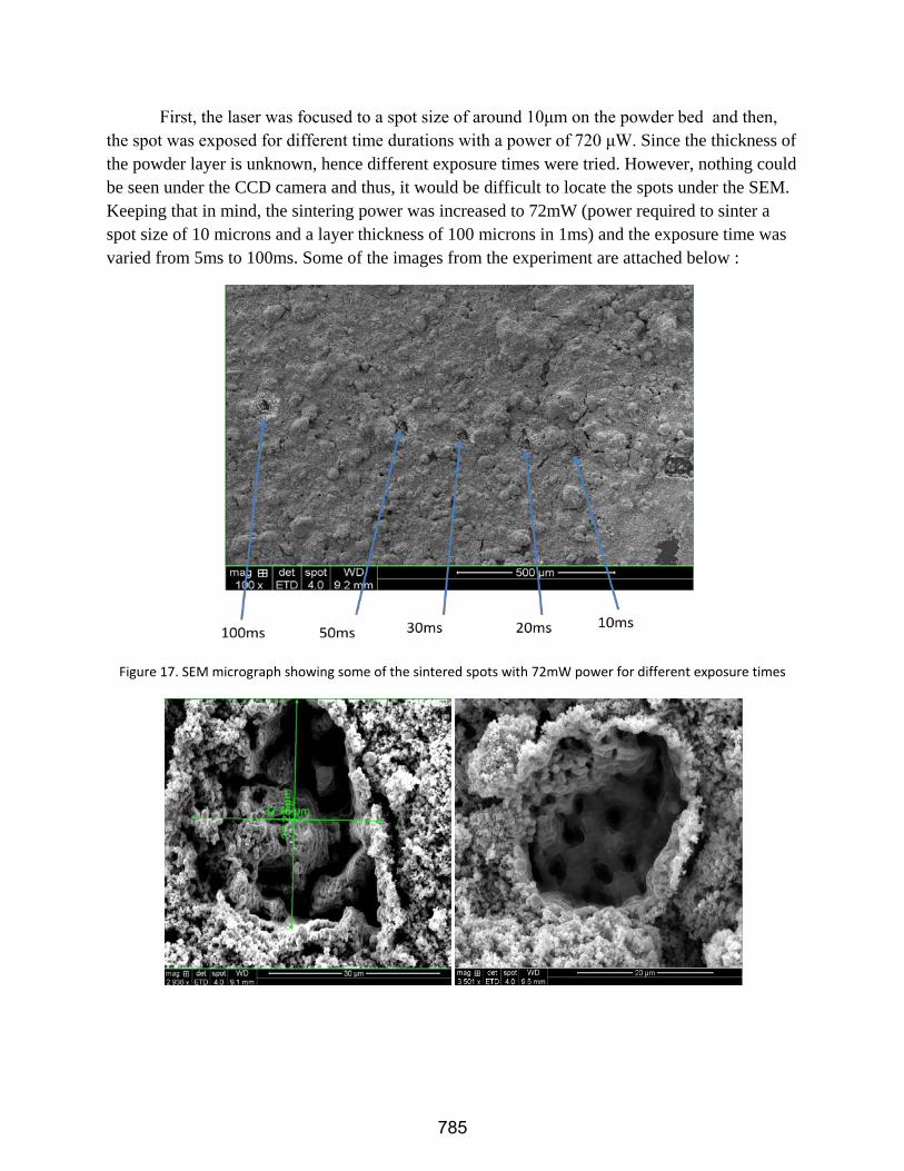
First, the laser was focused to a spot size of around 10μm on the powder bed and then, the spot was exposed for different time durations with a power of 720 μW. Since the thickness of the powder layer is unknown, hence different exposure times were tried. However, nothing could be seen under the CCD camera and thus, it would be difficult to locate the spots under the SEM. Keeping that in mind, the sintering power was increased to 72mW (power required to sinter a spot size of 10 microns and a layer thickness of 100 microns in 1ms) and the exposure time was varied from 5ms to 100ms. Some of the images from the experiment are attached below :
Figure 17. SEM micrograph showing some of the sintered spots with 72mW power for different exposure times
785
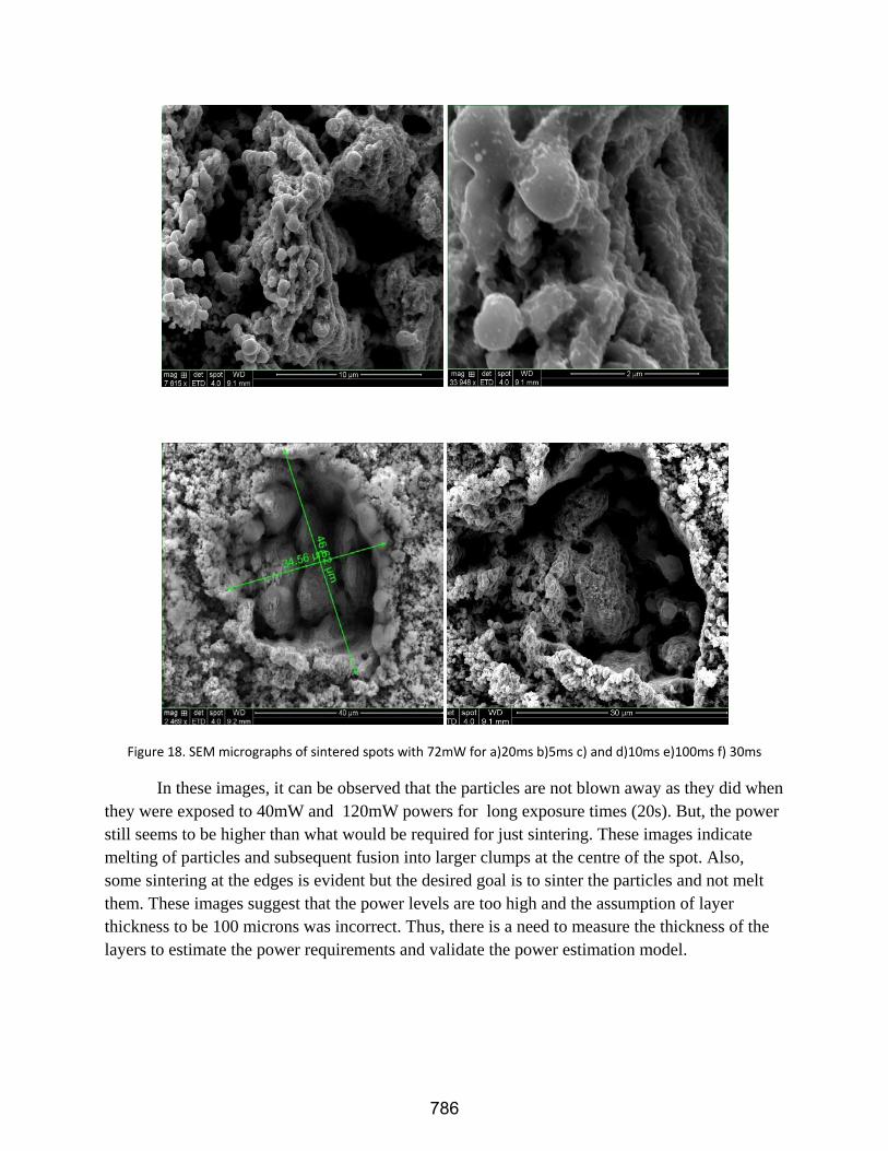
Figure 18. SEM micrographs of sintered spots with 72mW for a)20ms b)5ms c) and d)10ms e)100ms f) 30ms
In these images, it can be observed that the particles are not blown away as they did when they were exposed to 40mW and 120mW powers for long exposure times (20s). But, the power still seems to be higher than what would be required for just sintering. These images indicate melting of particles and subsequent fusion into larger clumps at the centre of the spot. Also, some sintering at the edges is evident but the desired goal is to sinter the particles and not melt them. These images suggest that the power levels are too high and the assumption of layer thickness to be 100 microns was incorrect. Thus, there is a need to measure the thickness of the layers to estimate the power requirements and validate the power estimation model.
786
Conclusion
Based on the observations of the experiments conducted, it is quite evident that there is a high extent of agglomeration in NPs and it needs to be dealt with suitably in order to spread a uniform layer of powder on the bed. A suitable alternative to reduce the extent of agglomeration is to use Cu NP inks as the extent of agglomeration in an ink is relatively lower and a thin layer of the particle can be spin coated on the substrate which would be very uniform. Secondly, in order to get estimates of the specific heat capacity, sintering temperature of the powders and know how the NPs behave thermally, Differential Scanning Calorimetry (DSC) will be performed. In order to track the changes in elemental composition of the sample as it is heated , X-Ray Photo Spectrometry can be performed at different conditions namely: at room temperature, at a temperature just above the exothermic peak temperature and at 1070°C. The composition of the sample at the three conditions can explain if there is any increase in oxygen content in the sample or not and what causes the reduction in weight of the sample. Ongoing research is focused towards 1) better documentation of sintering of powders with different powers , exposure times and known thickness of the powder layer , 2) to try Cu nano-inks for sintering, 3) designing an experiment for measuring the thermal conductivity of the sample which is another important parameter in the thermal modeling of the sintering process and 4) absorption spectroscopy to get the absorption spectrum of the Cu NPs at different wavelengths which will aid in selecting the laser for the system.
References
1. Yuan, M., D. Bourell, and T. Diller. Thermal conductivity measurements of polyamide 12. in In Proceedings of the Solid Freeform Fabrication Symposium. 2011.
2. Exner, H., et al. Selective laser micro sintering with a novel process. in Fourth International Symposium on Laser Precision Microfabrication. 2003. International Society for Optics and Photonics.
3. Scicolone, J., et al. Deagglomeration and mixing of nanoparticles. in annual PARTEC 2007 meeting, Paper. 2007.
4. Cheng, T., Y. Wu, and H. Chen, Effects of morphology on the radiative properties of internally mixed light absorbing carbon aerosols with different aging status. Optics express, 2014. 22(13): p. 15904-15917.
5. Pycnomatic ATC for solids and powders density. 2009. 6. Gibson, I. and D. Shi, Material properties and fabrication parameters in selective laser sintering
process. Rapid Prototyping Journal, 1997. 3(4): p. 129-136. 7. Ebert, R., et al. Process assembly for μm-scale SLS, reaction sintering, and CVD. in Fourth
International Symposium on laser Precision Microfabrication. 2003. International Society for Optics and Photonics.
8. Park, B.K., et al., Synthesis and size control of monodisperse copper nanoparticles by polyol method. Journal of colloid and interface science, 2007. 311(2): p. 417-424.
9. Zhang, H.-X., et al., Facile fabrication of ultrafine copper nanoparticles in organic solvent. Nanoscale research letters, 2009. 4(7): p. 705-708.
787
10. Taurozzi, J., V. Hackley, and M. Wiesner, Preparation of nanoparticle dispersions from powdered material using ultrasonic disruption. NIST Special Publication, 2012. 1200: p. 2.
11. Jang, S., et al., Sintering of inkjet printed copper nanoparticles for flexible electronics. Scripta Materialia, 2010. 62(5): p. 258-261.
12. Dewidar, M.M.A., Direct and indirect laser sintering of metals, 2002, University of Leeds. 13. Regenfuss, P., et al., Microparts by a novel modification of selective laser sintering. 14. Streek, A., et al. Laser micro sintering–a quality leap through improvement of powder packing. in
The Proceedings of the 19th Annual SFF Symposium. 2008. 15. Lee, J., D.-K. Kim, and W. Kang, Preparation of Cu nanoparticles from Cu powder dispersed in 2-
propanol by laser ablation. Bulletin of the Korean Chemical Society, 2006. 27(11): p. 1869-1872. 16. Tolochko, N.K., et al., Absorptance of powder materials suitable for laser sintering. Rapid
Prototyping Journal, 2000. 6(3): p. 155-161. 17. Instruments, T., DLP 5500 DLP 0.55 XGA Series 450 DMD, May 2015. 18. Zenou, M., et al., Laser sintering of copper nanoparticles. Journal of Physics D: Applied Physics,
2014. 47(2): p. 025501. 19. Kim, H.-S., et al., Intense pulsed light sintering of copper nanoink for printed electronics. Applied
Physics A, 2009. 97(4): p. 791-798. 20. Akbari, B., M.P. Tavandashti, and M. Zandrahimi, Particle Size Characterization of Nanoparticles–
A Practicalapproach. Iranian Journal of Materials Science and Engineering, 2011. 8(2): p. 48-56. 21. Sun, M.-s.M., J.J. Beaman, and J.W. Barlow. Parametric analysis of the selective laser sintering
process. in Proceedings of the Solid Freeform Fabrication Symposium, The University of Texas at Austin, Austin, TX. 1990. Citeseer.
22. Das, S., Physical aspects of process control in selective laser sintering of metals. Advanced Engineering Materials, 2003. 5(10): p. 701-711.
23. Zhang, Y.-L., et al., Designable 3D nanofabrication by femtosecond laser direct writing. Nano Today, 2010. 5(5): p. 435-448.
24. Theodorakos, I., et al., Selective laser sintering of Ag nanoparticles ink for applications in flexible electronics. Applied Surface Science, 2015. 336: p. 157-162.
25. Sih, S.S. and J.W. Barlow. The Measurement of the Thermal Properties and Absorptances of Powders Near Their Melting Temperatures. in Proceedings of the Solid Freeform Fabrication Symposium 1992. 1992. DTIC Document.
26. Kumar, S., Selective laser sintering: a qualitative and objective approach. JOM, 2003. 55(10): p. 43-47.
788