Δ Introduction to ΔΣ ModulatorsA very important parameter in Delta-Sigma modulators is the...
11
Introduction to ΔΣ Modulators Pietro Andreani Dept. of Electrical and Information Technology Lund University, Sweden Advanced AD/DA converters Introduction 2 Overview • Nyquist-rate vs. oversampled converters • Δ modulators • ΔΣ modulators • Higher-order ΔΣ modulators • Bandpass ΔΣ modulators • Multi-bit ΔΣ modulators • ΔΣ DACs • State-of-the-art and beyond Advanced AD/DA Converters Advanced AD/DA Converters Introduction 3 Nyquist-rate or oversampled? Data converters are roughly divided into two subgroups: Nyquist-rate and oversampled Nyquist-rate usually, the converter has no memory each input is processed independently of the other samples – the sampling rate can be theoretically as low as required by Nyquist’s criterion (i.e. at least twice the signal bandwidth) In these converters, linearity and accuracy is determined by the matching accuracy of the analog components used (resistors, capacitors, current sources, etc) – e.g. in an N-bit resistor-string DAC, matching must be better than 2 -N if the INL is to be below 0.5LSB Practical issues limit matching to 0.02% at best ENOB is 12b (but usually lower without extensive digital error correction) In applications such as digital audio (and other as well) at least 18 bits are required – integrating converters can deliver this, but need 2 N clock cycles for 1 conversion too slow for many applications! Advanced AD/DA Converters Introduction 4 Nyquist-rate or oversampled? Oversampled converters can go beyond 20b of resolution at reasonable conversion speed, by employing a much higher sampling rate (by a factor typically between 8 and 512) than required by Nyquist, while generating each output by utilizing all previous inputs (through feedback) Oversampling converters need a considerable amount of digital circuitry, besides some analog functions, and all functions must operate at the oversampling frequency However, the crucial point is that the accuracy of the analog functions is relaxed (compared to Nyquist-rate converters), while faster operation and digital circuitry take advantage of the increased scaling in CMOS processes – as a whole, oversampled converters are quite digital- friendly, and this explains their enormous popularity, which makes them more and more attractive for applications that were once the exclusive domain of Nyquist-rate converters
Transcript of Δ Introduction to ΔΣ ModulatorsA very important parameter in Delta-Sigma modulators is the...
Introduction to ΔΣ Modulators
Pietro AndreaniDept. of Electrical and Information Technology
Lund University, Sweden
Advanced AD/DA converters
Introduction 2
Overview
• Nyquist-rate vs. oversampled converters
• Δ modulators
• ΔΣ modulators
• Higher-order ΔΣ modulators
• Bandpass ΔΣ modulators
• Multi-bit ΔΣ modulators
• ΔΣ DACs
• State-of-the-art and beyond
Advanced AD/DA Converters
Advanced AD/DA Converters Introduction 3
Nyquist-rate or oversampled?
Data converters are roughly divided into two subgroups: Nyquist-rate and oversampled
Nyquist-rate usually, the converter has no memory each input is processed independently of the other samples – the sampling rate can be theoretically as low as required by Nyquist’s criterion (i.e. at least twice the signal bandwidth)
In these converters, linearity and accuracy is determined by the matching accuracy of the analog components used (resistors, capacitors, current sources, etc) – e.g. in an N-bit resistor-string DAC, matching must be better than 2-N if the INL is to be below 0.5LSB
Practical issues limit matching to 0.02% at best ENOB is 12b (but usually lower without extensive digital error correction)
In applications such as digital audio (and other as well) at least 18 bits are required – integrating converters can deliver this, but need 2N clock cycles for 1 conversion too slow for many applications!
Advanced AD/DA Converters Introduction 4
Nyquist-rate or oversampled?
Oversampled converters can go beyond 20b of resolution at reasonable conversion speed, by employing a much higher sampling rate (by a factor typically between 8 and 512) than required by Nyquist, while generating each output by utilizing all previous inputs (through feedback)
Oversampling converters need a considerable amount of digital circuitry, besides some analog functions, and all functions must operate at the oversampling frequency
However, the crucial point is that the accuracy of the analog functions is relaxed (compared to Nyquist-rate converters), while faster operation and digital circuitry take advantage of the increased scaling in CMOS processes – as a whole, oversampled converters are quite digital-friendly, and this explains their enormous popularity, which makes them more and more attractive for applications that were once the exclusive domain of Nyquist-rate converters
Advanced AD/DA Converters Introduction 5
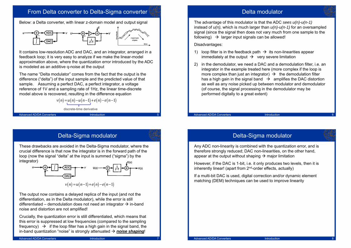
From Delta converter to Delta-Sigma converter
Below: a Delta converter, with linear z-domain model and output signal
It contains low-resolution ADC and DAC, and an integrator, arranged in a feedback loop; it is very easy to analyze if we make the linear-model approximation above, where the quantization error introduced by the ADC is modeled as an additive q-noise at the output
The name “Delta modulator” comes from the fact that the output is the difference (“delta”) of the input sample and the predicted value of that sample. Assuming a perfect DAC, a perfect integrator, a voltage reference of 1V and a sampling rate of 1Hz, the linear time-discrete model above is recovered, resulting in the difference equation
( ) ( ) ( ) ( ) ( )1 1v n u n u n e n e n= − − + − −
discrete-time derivativeAdvanced AD/DA Converters Introduction 6
Delta modulator
The advantage of this modulator is that the ADC sees u(n)-u(n-1) instead of u(n), which is much larger than u(n)-u(n-1) for an oversampled signal (since the signal then does not vary much from one sample to the following) larger input signals can be allowed!
Disadvantages:
1) loop filter is in the feedback path its non-linearities appear immediately at the output very severe limitation
2) in the demodulator, we need a DAC and a demodulation filter, i.e. an integrator in the example treated here (more complex if the loop is more complex than just an integrator) the demodulation filter has a high gain in the signal band amplifies the DAC distortion as well as any noise picked up between modulator and demodulator (of course, the signal processing in the demodulator may be performed digitally to a great extent)
Advanced AD/DA Converters Introduction 7
Delta-Sigma modulator
These drawbacks are avoided in the Delta-Sigma modulator, where the crucial difference is that now the integrator is in the forward path of the loop (now the signal “delta” at the input is summed (“sigma”) by the integrator)
The output now contains a delayed replica of the input (and not the differentiation, as in the Delta modulator), while the error is still differentiated – demodulation does not need an integrator in-band noise and distortion are not amplified!
Crucially, the quantization error is still differentiated, which means that this error is suppressed at low frequencies (compared to the sampling frequency) if the loop filter has a high gain in the signal band, the in-band quantization “noise” is strongly attenuated noise shaping!
( ) ( ) ( ) ( )1 1v n u n e n e n= − + − −
Advanced AD/DA Converters Introduction 8
Delta-Sigma modulator
Any ADC non-linearity is combined with the quantization error, and is therefore strongly reduced; DAC non-linearities, on the other hand, appear at the output without shaping major limitation
However, if the DAC is 1-bit, i.e. it only produces two levels, then it is inherently linear! (apart from 2nd-order effects, actually)
If a multi-bit DAC is used, digital correction and/or dynamic element matching (DEM) techniques can be used to improve linearity
Advanced AD/DA Converters Introduction 9
Noise shaping
Most of the q-noise is shifted towards high frequencies (where it can be filtered off), removing it from the signal band SNR largely improved
the ENOB can greatly exceed what would be allowed in terms of pure component matching
Advanced AD/DA Converters Introduction 10
Noise shapingThe power spectral density of the q-noise is found as
where is the PSD of the q-error (q-noise) of the internal ADC
For “busy” input signals, the q-noise is approximately white, with power
where Δ is the quantization step; since the q-noise PSD is white between DC and fs/2, we obtain
The function is the so-called noise transfer function (NTF) of the modulator, and is obviously a high-pass filter function
q-noise is suppressed at and near DC
( ) ( ) ( ) ( ) ( ) ( ) ( ) ( ) ( )211 1 2sinq eq n e n e n Q z z E z S f fT S fπ−= − − → = − → = ⎡ ⎤⎣ ⎦( )eS f
2 2 12rmse = Δ
( )2
6es
S ff
Δ=
( )11 z−−
Advanced AD/DA Converters Introduction 11
Oversampling ratio
A very important parameter in Delta-Sigma modulators is the oversampling ratio (OSR) – if fB is the maximum frequency of the input signal, the OSR is defined as
The OSR defines how much faster the modulator is operated, compared to a Nyquist converter (which ideally has OSR=1)
Integrating the q-noise over the signal band yields, for OSR >> 1:
As expected, q-noise decreases with increasing OSR; for a doubling of the OSR, q-noise power drops by a factor 8 = 9dB = 1.5b, which is good (but not very good!)
22
Nyq s s
B B B
f f fOSRf f f
= = =
( ) ( )
( )
222
0 0
2 2 2 2 2 22 3 2 32
3 30
2sin2
4 8 42 2 3 3 3
B B
B
f frmsrms q
s
frms rms rms rmsB B
s s s
eq S f df fT dff
e e e ef T ffT dff f f OSR
π
π πππ
= = ⎡ ⎤⎣ ⎦
≈ = = =⋅
∫ ∫
∫
Advanced AD/DA Converters Introduction 12
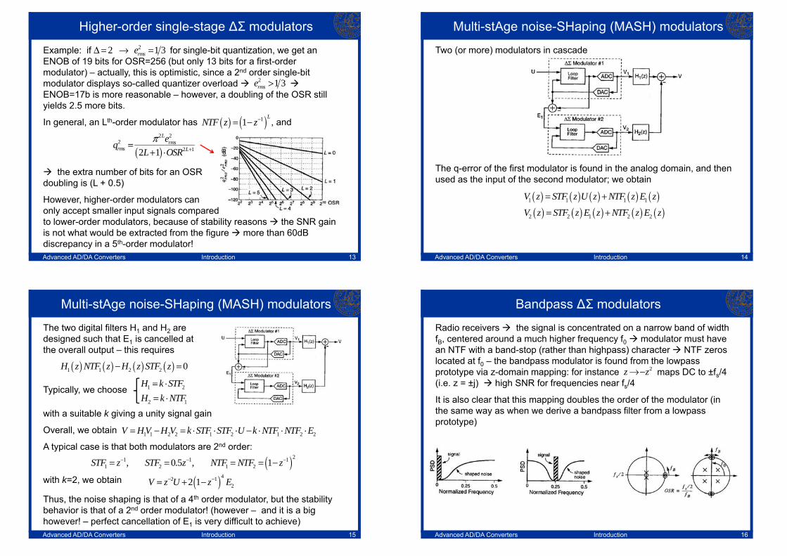
Higher-order single-stage ΔΣ modulators
A way of improving the SNR of the modulator, apart from increasing the OSR, is to use a higher-order loop filter; e.g., the 2nd-order below
Again, a linear analysis yields , and therefore the NTF is now a 2nd-order highpass filter:
which yields the q-noise over the signal band
In this case, doubling the OSR yields 2.5 bits of additional resolution, which is much better!
( ) ( ) ( ) ( )21 11V z z U z z E z− −= + −
( ) ( ) ( ) ( )2 41 21 2sinj fTNTF z z NTF e fTπ π−= − → = ⎡ ⎤⎣ ⎦
4 22
55rms
rmseq
OSRπ=⋅
Advanced AD/DA Converters Introduction 13
Higher-order single-stage ΔΣ modulators
Example: if for single-bit quantization, we get an ENOB of 19 bits for OSR=256 (but only 13 bits for a first-order modulator) – actually, this is optimistic, since a 2nd order single-bit modulator displays so-called quantizer overload ENOB=17b is more reasonable – however, a doubling of the OSR still yields 2.5 more bits.
In general, an Lth-order modulator has , and
the extra number of bits for an OSR doubling is (L + 0.5)
However, higher-order modulators can only accept smaller input signals compared to lower-order modulators, because of stability reasons the SNR gain is not what would be extracted from the figure more than 60dB discrepancy in a 5th-order modulator!
( )2 2
22 12 1
Lrms
rms L
eqL OSR
π+=
+ ⋅
22 1 3rmseΔ = → =
2 1 3rmse >
( ) ( )11L
NTF z z−= −
Advanced AD/DA Converters Introduction 14
Multi-stAge noise-SHaping (MASH) modulators
Two (or more) modulators in cascade
The q-error of the first modulator is found in the analog domain, and then used as the input of the second modulator; we obtain
( ) ( ) ( ) ( ) ( )( ) ( ) ( ) ( ) ( )
1 1 1 1
2 2 1 2 2
V z STF z U z NTF z E z
V z STF z E z NTF z E z
= +
= +
Advanced AD/DA Converters Introduction 15
Multi-stAge noise-SHaping (MASH) modulators
The two digital filters H1 and H2 are designed such that E1 is cancelled at the overall output – this requires
Typically, we choose
with a suitable k giving a unity signal gain
Overall, we obtain
A typical case is that both modulators are 2nd order:
with k=2, we obtain
1 1 2 2 1 2 1 2 2V HV H V k STF STF U k NTF NTF E= − = ⋅ ⋅ ⋅ − ⋅ ⋅ ⋅
( ) ( ) ( ) ( )1 1 2 2 0H z NTF z H z STF z− =
1 2
2 1
H k STFH k NTF
= ⋅= ⋅
( )21 1 11 2 1 2, 0.5 , 1STF z STF z NTF NTF z− − −= = = = −
( )42 122 1V z U z E− −= + −
Thus, the noise shaping is that of a 4th order modulator, but the stability behavior is that of a 2nd order modulator! (however – and it is a big however! – perfect cancellation of E1 is very difficult to achieve)
Advanced AD/DA Converters Introduction 16
Bandpass ΔΣ modulators
Radio receivers the signal is concentrated on a narrow band of width fB, centered around a much higher frequency f0 modulator must have an NTF with a band-stop (rather than highpass) character NTF zeros located at f0 – the bandpass modulator is found from the lowpass prototype via z-domain mapping: for instance maps DC to ±fs/4 (i.e. z = ±j) high SNR for frequencies near fs/4
It is also clear that this mapping doubles the order of the modulator (in the same way as when we derive a bandpass filter from a lowpass prototype)
2z z→−
Advanced AD/DA Converters Introduction 17
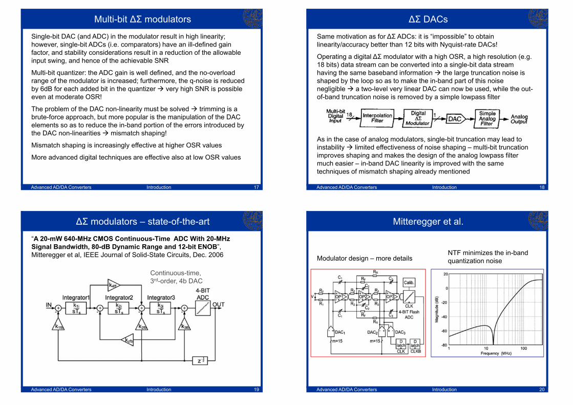
Multi-bit ΔΣ modulators
Single-bit DAC (and ADC) in the modulator result in high linearity; however, single-bit ADCs (i.e. comparators) have an ill-defined gain factor, and stability considerations result in a reduction of the allowable input swing, and hence of the achievable SNR
Multi-bit quantizer: the ADC gain is well defined, and the no-overload range of the modulator is increased; furthermore, the q-noise is reduced by 6dB for each added bit in the quantizer very high SNR is possible even at moderate OSR!
The problem of the DAC non-linearity must be solved trimming is a brute-force approach, but more popular is the manipulation of the DAC elements so as to reduce the in-band portion of the errors introduced by the DAC non-linearities mismatch shaping!
Mismatch shaping is increasingly effective at higher OSR values
More advanced digital techniques are effective also at low OSR values
Advanced AD/DA Converters Introduction 18
ΔΣ DACs
Same motivation as for ΔΣ ADCs: it is “impossible” to obtain linearity/accuracy better than 12 bits with Nyquist-rate DACs!
Operating a digital ΔΣ modulator with a high OSR, a high resolution (e.g. 18 bits) data stream can be converted into a single-bit data stream having the same baseband information the large truncation noise is shaped by the loop so as to make the in-band part of this noise negligible a two-level very linear DAC can now be used, while the out-of-band truncation noise is removed by a simple lowpass filter
As in the case of analog modulators, single-bit truncation may lead to instability limited effectiveness of noise shaping – multi-bit truncation improves shaping and makes the design of the analog lowpass filter much easier – in-band DAC linearity is improved with the same techniques of mismatch shaping already mentioned
Advanced AD/DA Converters Introduction 19
ΔΣ modulators – state-of-the-art
“A 20-mW 640-MHz CMOS Continuous-Time ADC With 20-MHz Signal Bandwidth, 80-dB Dynamic Range and 12-bit ENOB”, Mitteregger et al, IEEE Journal of Solid-State Circuits, Dec. 2006
Continuous-time, 3rd-order, 4b DAC
Advanced AD/DA Converters Introduction 20
Mitteregger et al.
Modulator design – more detailsNTF minimizes the in-band quantization noise
Advanced AD/DA Converters Introduction 21
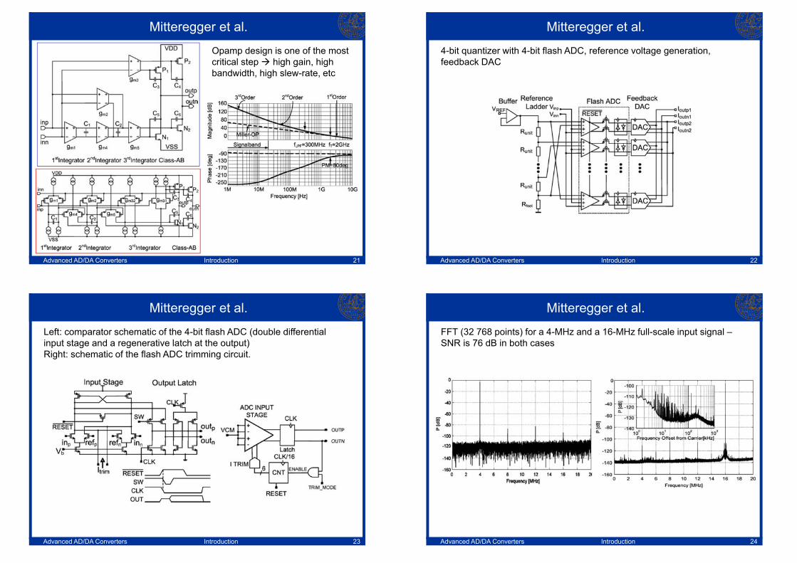
Mitteregger et al.
Opamp design is one of the most critical step high gain, high bandwidth, high slew-rate, etc
Advanced AD/DA Converters Introduction 22
Mitteregger et al.
4-bit quantizer with 4-bit flash ADC, reference voltage generation,feedback DAC
Advanced AD/DA Converters Introduction 23
Mitteregger et al.
Left: comparator schematic of the 4-bit flash ADC (double differential input stage and a regenerative latch at the output)Right: schematic of the flash ADC trimming circuit.
Advanced AD/DA Converters Introduction 24
Mitteregger et al.
FFT (32 768 points) for a 4-MHz and a 16-MHz full-scale input signal –SNR is 76 dB in both cases
Advanced AD/DA Converters Introduction 25
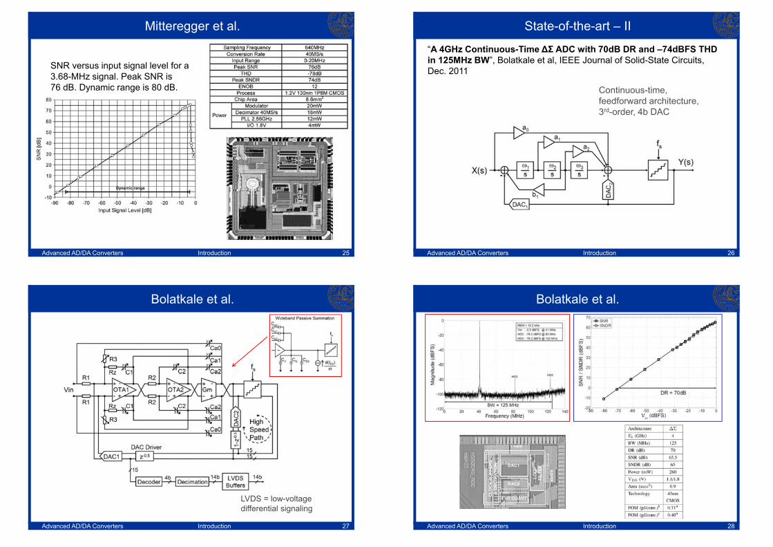
Mitteregger et al.
SNR versus input signal level for a 3.68-MHz signal. Peak SNR is76 dB. Dynamic range is 80 dB.
Advanced AD/DA Converters Introduction 26
State-of-the-art – II
“A 4GHz Continuous-Time ΔΣ ADC with 70dB DR and –74dBFS THD in 125MHz BW”, Bolatkale et al, IEEE Journal of Solid-State Circuits, Dec. 2011
Continuous-time, feedforward architecture, 3rd-order, 4b DAC
Advanced AD/DA Converters Introduction 27
Bolatkale et al.
LVDS = low-voltage differential signaling
Advanced AD/DA Converters Introduction 28
Bolatkale et al.
Advanced AD/DA Converters Introduction 29
ΔΣ modulators – state-of-the-art – III
“A 15mW 3.6GS/s CT-ΔΣ ADC with 36MHz Bandwidth and 83dB DR in 90nm CMOS”, Shettigar and Pavan, ISSCC 2012, Feb. 2012; JSSC Dec. 2012.
CT, 4th-order, 1b DACs
1st DAC with FIR reduces sensitivity to clock jitter, and relaxes demand on loop filter linearity
Advanced AD/DA Converters Introduction 30
ΔΣ modulators – state-of-the-art – III
a) feedforward-compensated 2-stage opampsb) quantizer
Advanced AD/DA Converters Introduction 31
ΔΣ modulators – state-of-the-art – III
Advanced AD/DA Converters Introduction 32
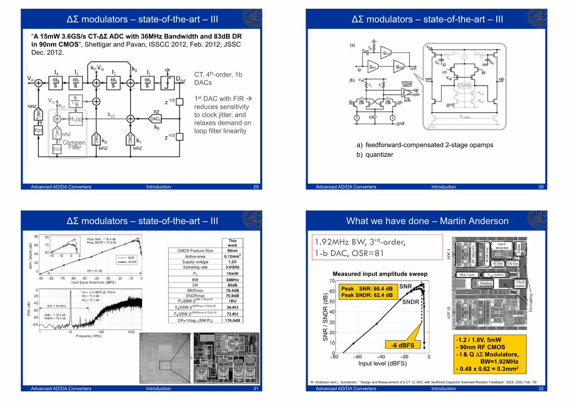
What we have done – Martin Anderson
SN
R /
SN
DR
(dB
)
SNR
SNDR
Peak SNR: 66.4 dBPeak SNDR: 62.4 dB
-6 dBFS
Input level (dBFS)
Measured input amplitude sweep
-1.2 / 1.8V, 5mW- 90nm RF CMOS- I & Q ΔΣ Modulators,
BW=1.92MHz- 0.48 x 0.62 = 0.3mm2
M. Anderson and L. Sundström, ” Design and Measurement of a CT ΔΣ ADC with Switched-Capacitor Switched-Resistor Feedback”, IEEE JSSC Feb. ’09
1.92MHz BW, 3rd-order, 1-b DAC, OSR=81
Advanced AD/DA Converters Introduction 33
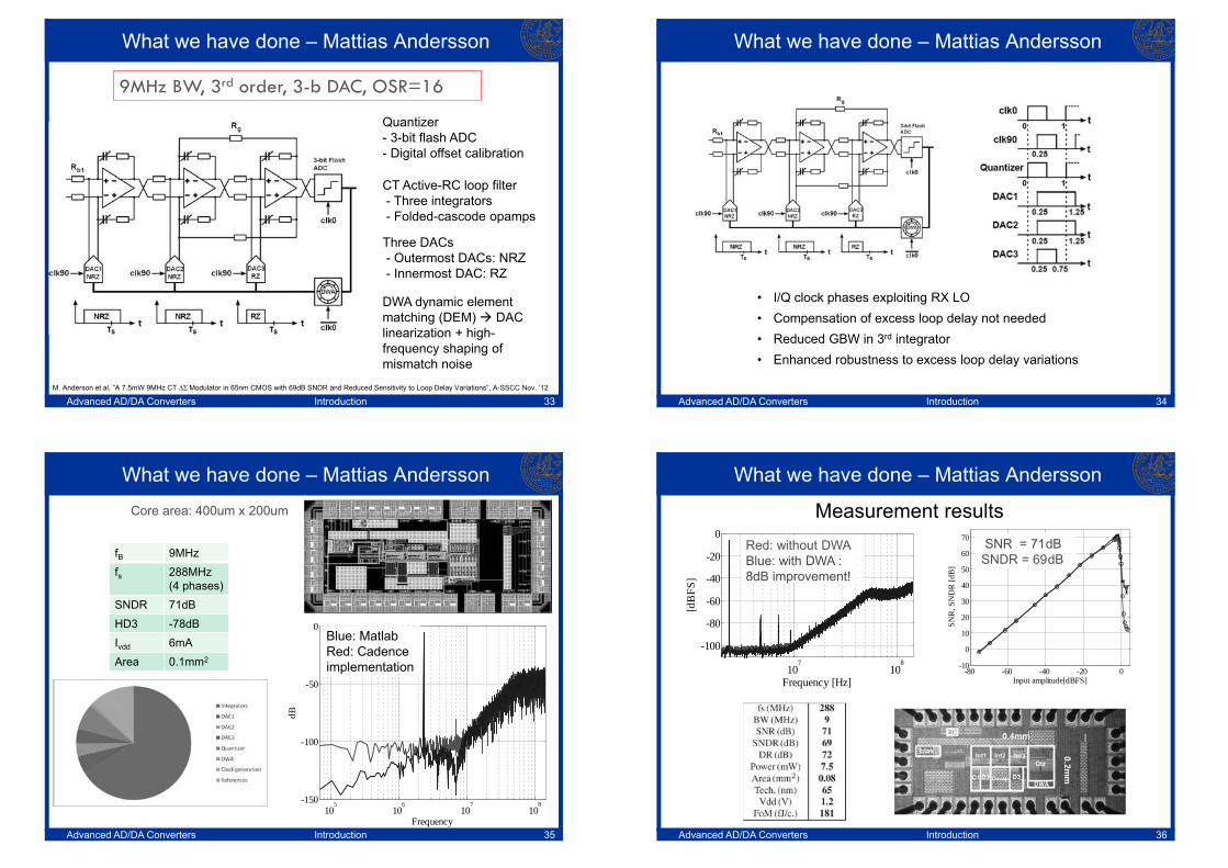
What we have done – Mattias Andersson
CT Active-RC loop filter- Three integrators - Folded-cascode opamps
Three DACs- Outermost DACs: NRZ- Innermost DAC: RZ
Quantizer- 3-bit flash ADC- Digital offset calibration
DWA dynamic element matching (DEM) DAC linearization + high-frequency shaping of mismatch noise
9MHz BW, 3rd order, 3-b DAC, OSR=16
M. Anderson et al, ”A 7.5mW 9MHz CT ΔΣ Modulator in 65nm CMOS with 69dB SNDR and Reduced Sensitivity to Loop Delay Variations”, A-SSCC Nov. ’12
Advanced AD/DA Converters Introduction 34
What we have done – Mattias Andersson
• I/Q clock phases exploiting RX LO• Compensation of excess loop delay not needed • Reduced GBW in 3rd integrator• Enhanced robustness to excess loop delay variations
Advanced AD/DA Converters Introduction 35
What we have done – Mattias Andersson
105
106
107
108-150
-100
-50
0
dB
Frequency
Blue: Matlab Red: Cadence implementation
fB 9MHzfs 288MHz
(4 phases)SNDR 71dBHD3 -78dBIvdd 6mAArea 0.1mm2
Core area: 400um x 200um
Advanced AD/DA Converters Introduction 36
What we have done – Mattias Andersson
-80 -60 -40 -20 0-10
0
10
20
30
40
50
60
70
Input amplitude[dBFS]
SNR
, SN
DR
[dB
]
SNR = 71dBSNDR = 69dB
107
108
-100
-80
-60
-40
-20
0
[dB
FS]
Frequency [Hz]
Red: without DWABlue: with DWA : 8dB improvement!
Measurement results
Advanced AD/DA Converters Introduction 37
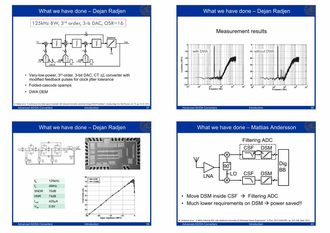
What we have done – Dejan Radjen
• Very-low-power, 3rd-order, 3-bit DAC, CT ΔΣ converter with modified feedback pulses for clock jitter tolerance
• Folded-cascode opamps
• DWA DEM
125kHz BW, 3rd order, 3-b DAC, OSR=16
D. Radjen et al, ”A continuous time delta-sigma modulator with reduced clock jitter sensitivity through DSCR feedback”, Analog Integr Circ Sig Process, vol. 73, pp. 21-31, 2013
Advanced AD/DA Converters Introduction 38
What we have done – Dejan Radjen
with DWA without DWA
Measurement results
Advanced AD/DA Converters Introduction 39
What we have done – Dejan Radjen
fB 125kHzfs 4MHzSNDR 70dBHNR 74dBIvdd 420μAVdd 0.9V
Advanced AD/DA Converters Introduction 40
What we have done – Mattias Andersson
M. Anderson et al, ” A 9MHz Filtering ADC with Additional 2nd-order ΔΣ Modulator Noise Suppression”, in Proc. 2013 ESSCIRC, pp. 323–326, Sept. 2013
• Move DSM inside CSF Filtering ADC• Much lower requirements on DSM power saved!!
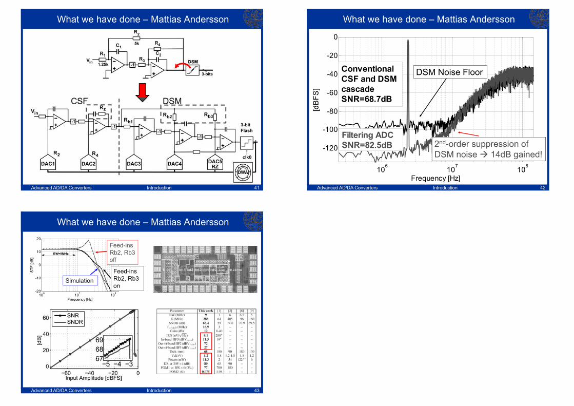
Advanced AD/DA Converters Introduction 41
What we have done – Mattias Andersson
Advanced AD/DA Converters Introduction 42
What we have done – Mattias Andersson
106 107 108
-120
-100
-80
-60
-40
-20
0
[dB
FS]
Frequency [Hz]
ConventionalCSF and DSMcascadeSNR=68.7dB
Filtering ADCSNR=82.5dB
DSM Noise Floor
2nd-order suppression of DSM noise 14dB gained!
Advanced AD/DA Converters Introduction 43
What we have done – Mattias Andersson
106 107 108-20
-10
0
10
20
Frequency [Hz]
STF
[dB
]
BW=9MHz
Feed-insRb2, Rb3 off
SimulationFeed-ins Rb2, Rb3 on