Μ D 12.08.2013 Embedded Systems Page 1 C166-Core Port 5 Port 3 CPU Dual Port RAM 2 KByte Interrupt...
38
µ D 04EI 12.08.2013 Embedded Systems Page 1 164C L XTAL C166- C166- Core Core Port 5 Port 3 CPU Dual Port RAM 2 KByte Interrupt Controller Watchdog Peripheral Data External Instr./Data Instr./Data USART ASC BRG GPT1 16 16 16 16 32 PEC 64 K ROM (C164 CI-8RM) or OTP (C164CI-8EM) Interrupt Bus Data Data Port 8 BRG SSC Sync. Channe l (SPI) PLL-Oscillator prog. Multiplier: 0.5; 1; 1.5; 2; 2.5; 3; 4; 5 XBUS (16-bit NON MUX Data / Addresses) T2 T4 T3 13 ext. IR Full-CAN Interface V2.0B active RTC 10-Bit ADC Timer 7 Timer 8 Port 1 Timer 13 1 Comp. Channel 3/6 CAPCOM Channels CAPCOM6 Unit for PWM Generation 8 9 4 16 6 16 Port 4 8-Channels External Bus 8/16 bit MUX only & XBUS Control CAPCOM 2 8-Channel C164CI - the Peripheral devices P4.6/ CAN TxD P4.5/ CAN RxD Port 0
-
Upload
anabel-richardson -
Category
Documents
-
view
219 -
download
0
Transcript of Μ D 12.08.2013 Embedded Systems Page 1 C166-Core Port 5 Port 3 CPU Dual Port RAM 2 KByte Interrupt...
µD
04EI
12.08.2013 Embedded Systems Page 1
164CL
XTAL
C166-CoreC166-Core
Port 5 Port 3
CPU
Dua
l Por
t
RAM
2 KByte
Interrupt Controller
Watchdog
Peripheral Data
External Instr./Data
Instr./Data
USART
ASC
BRG
GPT1
16
16
16
1632
PEC
64 K ROM
(C164 CI-8RM)or
OTP(C164CI-8EM)
Interrupt Bus
Data
Data
Port 8
BRG
SSC
Sync. Channel(SPI)
PLL-Oscillatorprog. Multiplier:
0.5; 1; 1.5; 2;2.5; 3; 4; 5
XB
US
(16-
bit N
ON
MU
X D
ata
/ Add
ress
es)
T2
T4
T3
13 ext. IR
Full-CANInterfaceV2.0Bactive
RTC
10-BitADC
Tim
er 7
Tim
er 8
Port 1
Tim
er 1
3
1 Comp.Channel
3/6 CAPCOMChannels
CAPCOM6 Unit forPWM Generation
8 9 4 16
6
16
Port 4
8-Channels
External Bus8/16 bit
MUX only&
XBUSControl
CAPCOM 2
8-Channel
C164CI - the Peripheral devices
P4.6/ CAN TxD
P4.5/ CANRxD
Port
0
µD
04EI
12.08.2013 Embedded Systems Page 2
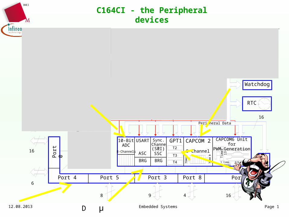
Overview of the I/O-PortsOverview of the I/O-Ports
• The Port-pins provide the connection to the ‚outside world‘
– the C164CI has got 59 Pins for port-connections:• 4 8-Bit-Ports: PORT0 as P0H and P0L; PORT1 as P1H and P1L.• 1 9-Bit-Port: PORT3 as P3.• 1 6-Bit-Port: PORT4 as P4.• 1 4-Bit-Port: PORT8 as P8.• 1 8-Bit-Port. PORT5 as P5 usable only as input.
• All port-connections may be adressed separtely bitwise.
• All I/O-lines are indepently programmable as Input - resp. output. via a direction selection register
• The port-connections are equipped with one or more alternative functions (Periphery or BUS).
• Each port is protected via fast diods.• Some ports additionally provide to be configured as buffered
“Open-Drain”-Outputs (P3 and P8 for C164CI).• Some ports provide a special treshold rating as CMOS-level (P3 and
P8 for C164CI) beside of the qualification of the input levels as TTL-signal
µD
04EI
12.08.2013 Embedded Systems Page 3
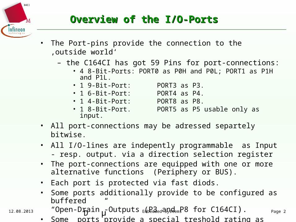
Overview of the port structure Overview of the port structure
DirectionRegister
AlternateOutput
AlternateEnable
Read
ClockAlternate Input
Inte
rnal
Bus
Buffer
Mux
Mux
OutputLatch
Write
Buffer
InputLatch
Open DrainControl
VCC
Vss
Port Pin
ESD structure
Ports Dave
µD
04EI
12.08.2013 Embedded Systems Page 4
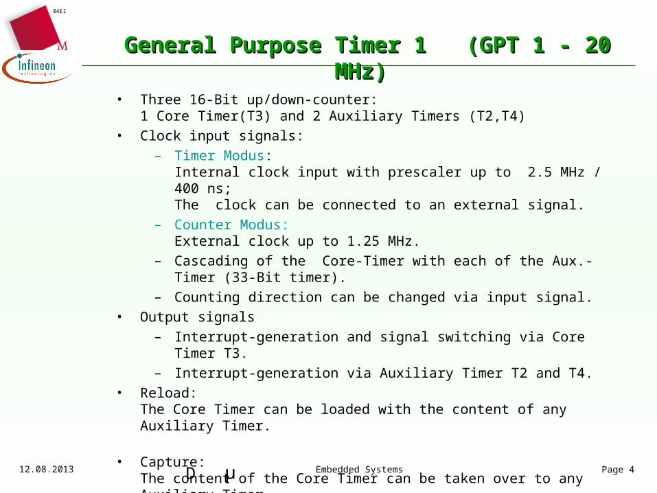
General Purpose Timer 1 (GPT 1 - 20 MHz) General Purpose Timer 1 (GPT 1 - 20 MHz)
• Three 16-Bit up/down-counter:1 Core Timer(T3) and 2 Auxiliary Timers (T2,T4)
• Clock input signals:– Timer Modus:
Internal clock input with prescaler up to 2.5 MHz / 400 ns; The clock can be connected to an external signal.
– Counter Modus: External clock up to 1.25 MHz.
– Cascading of the Core-Timer with each of the Aux.-Timer (33-Bit timer).
– Counting direction can be changed via input signal.• Output signals
– Interrupt-generation and signal switching via Core Timer T3.– Interrupt-generation via Auxiliary Timer T2 and T4.
• Reload:The Core Timer can be loaded with the content of any Auxiliary Timer.
• Capture:The content of the Core Timer can be taken over to any Auxiliary Timer
µD
04EI
12.08.2013 Embedded Systems Page 5
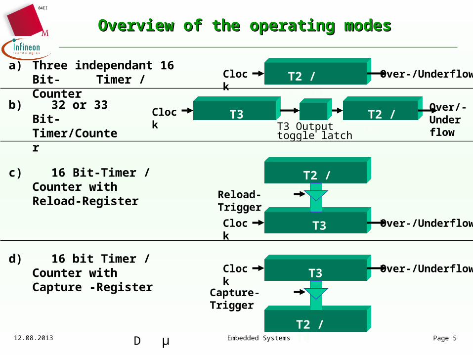
T2 / T3 /T4 Over-/UnderflowClocka) Three independant 16 Bit-
Timer / Counter
T2 / T4Over/-Underflow
b) 32 or 33 Bit- Timer/Counter T3Clock
T3 Outputtoggle latch
T2 / T4
T3 Over-/UnderflowClock
Capture-Trigger
T2 / T4
d) 16 bit Timer / Counter with Capture -Register
T2 / T4c) 16 Bit-Timer / Counter with Reload-Register
T3 Over-/UnderflowClock
Reload-Trigger
Overview of the operating modesOverview of the operating modes
µD
04EI
12.08.2013 Embedded Systems Page 6
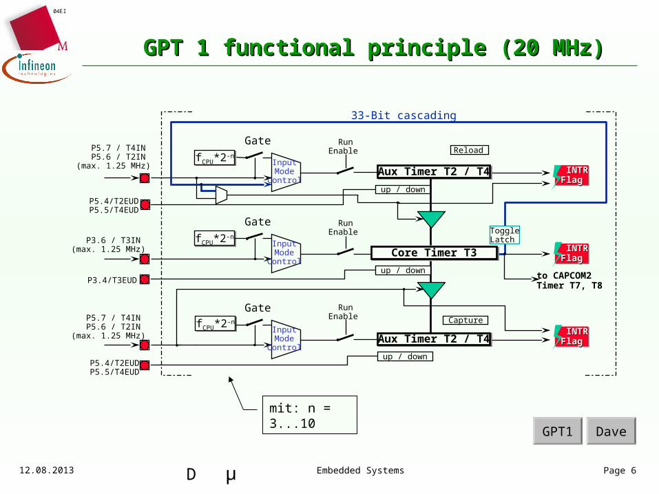
GPT 1 functional principle (20 MHz)GPT 1 functional principle (20 MHz)
fCPU*2-nfCPU*2-n
fCPU*2-nfCPU*2-n
mit: n = 3...10
GPT1 Dave
Gate
InputMode
Control Core Timer T3 Core Timer T3
ToggleLatch
INTRINTR Flag Flag INTRINTR Flag Flag
Gate
InputMode
ControlAux Timer T2 / T4Aux Timer T2 / T4
Capture
RunEnable
INTRINTR Flag Flag INTRINTR Flag Flag
Gate
InputMode
ControlAux Timer T2 / T4Aux Timer T2 / T4
up / down
RunEnable
INTRINTR Flag Flag INTRINTR Flag Flag
Reload Run
Enable fCPU*2-nfCPU*2-n
33-Bit cascading
up / down
up / down
P5.7 / T4INP5.6 / T2IN
(max. 1.25 MHz)
P5.7 / T4INP5.6 / T2IN
(max. 1.25 MHz)
P3.6 / T3IN(max. 1.25 MHz)
P5.4/T2EUDP5.5/T4EUD
P5.4/T2EUDP5.5/T4EUD
P3.4/T3EUD to CAPCOM2Timer T7, T8
µD
04EI
27.9.2009 Embedded Systems Page 7
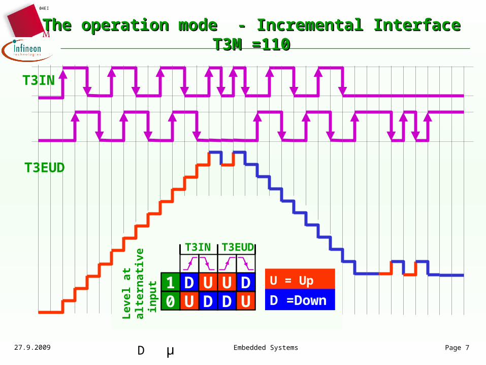
The operation mode - Incremental Interface T3M =110The operation mode - Incremental Interface T3M =110
U = Up
D =DownD
T3IN T3EUD
D DD1
0 UU U
ULev
el a
t
alte
rnat
ive
inp
ut
T3IN
T3EUD
µD
04EI
12.08.2013 Embedded Systems Page 8
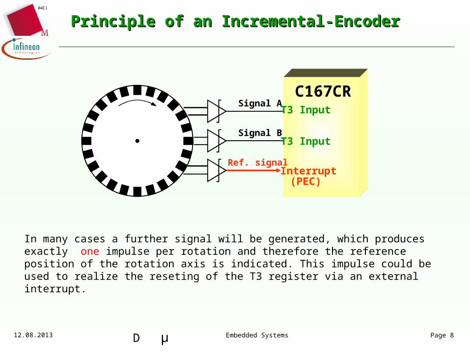
Principle of an Incremental-EncoderPrinciple of an Incremental-Encoder
Signal B
Signal A
Ref. signal
T3 Input
T3 Input
Interrupt(PEC)
C167CR
In many cases a further signal will be generated, which produces exactly one impulse per rotation and therefore the reference position of the rotation axis is indicated. This impulse could be used to realize the reseting of the T3 register via an external interrupt.
µD
04EI
12.08.2013 Embedded Systems Page 9
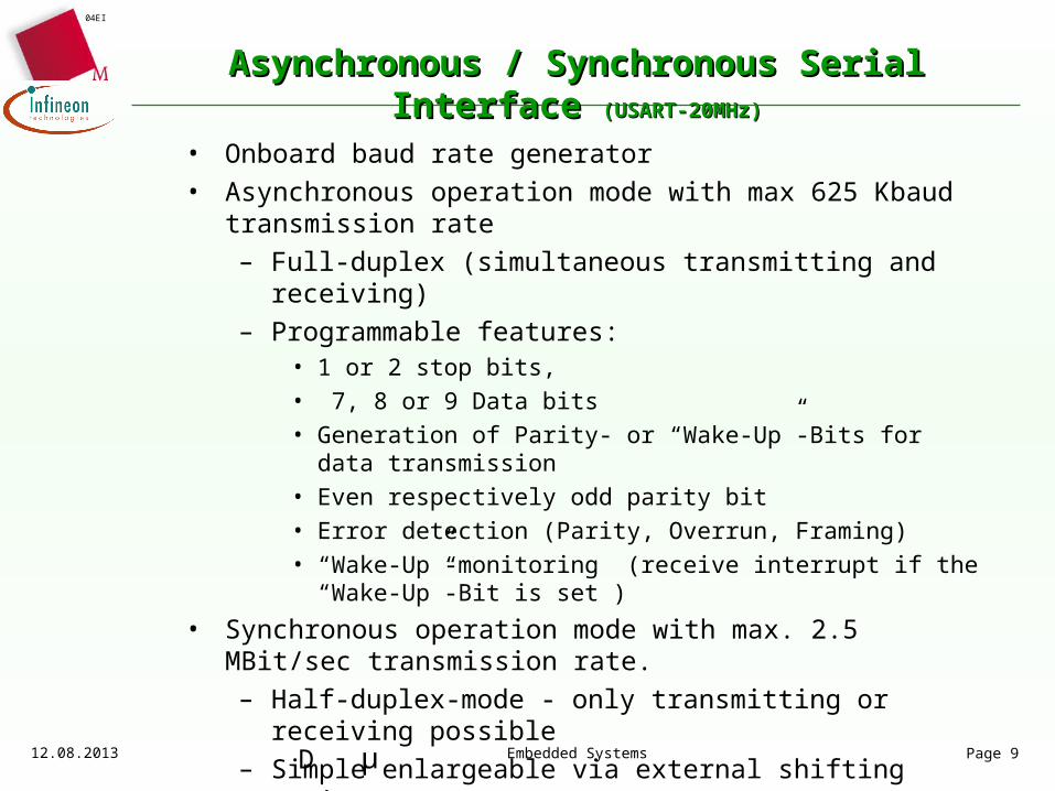
Asynchronous / Synchronous Serial Interface Asynchronous / Synchronous Serial Interface (USART-20MHz)(USART-20MHz)
• Onboard baud rate generator
• Asynchronous operation mode with max 625 Kbaudtransmission rate
– Full-duplex (simultaneous transmitting and receiving)
– Programmable features:• 1 or 2 stop bits,• 7, 8 or 9 Data bits• Generation of Parity- or “Wake-Up”-Bits for data transmission • Even respectively odd parity bit• Error detection (Parity, Overrun, Framing)• “Wake-Up”-monitoring (receive interrupt if the “Wake-Up”-Bit is
set )
• Synchronous operation mode with max. 2.5 MBit/sec transmission rate.
– Half-duplex-mode - only transmitting or receiving possible
– Simple enlargeable via external shifting registers.
– Overrun-errors are recognized.
µD
04EI
12.08.2013 Embedded Systems Page 10
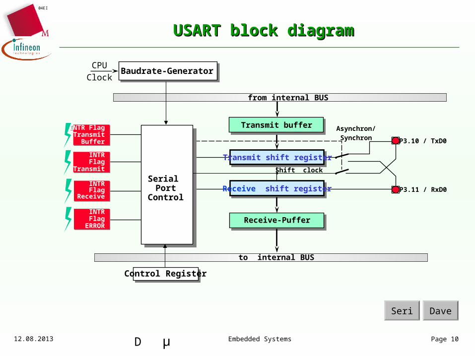
INTR Flag
Transmit
INTR Flag
Transmit
INTR Flag
Receive
INTR Flag
Receive
INTR Flag
ERROR
INTR Flag
ERROR
to internal BUS
Control Register
Serial Port
Control
Transmit shift register
Receive shift register
Receive-Puffer
from internal BUS
Shift clock
Asynchron/
Synchron
USART block diagramUSART block diagram
P3.11 / RxD0
P3.10 / TxD0
Baudrate-GeneratorCPU
Clock
Transmit buffer
Seri Dave
INTR FlagTransmit
Buffer
INTR FlagTransmit
Buffer
µD
04EI
12.08.2013 Embedded Systems Page 11
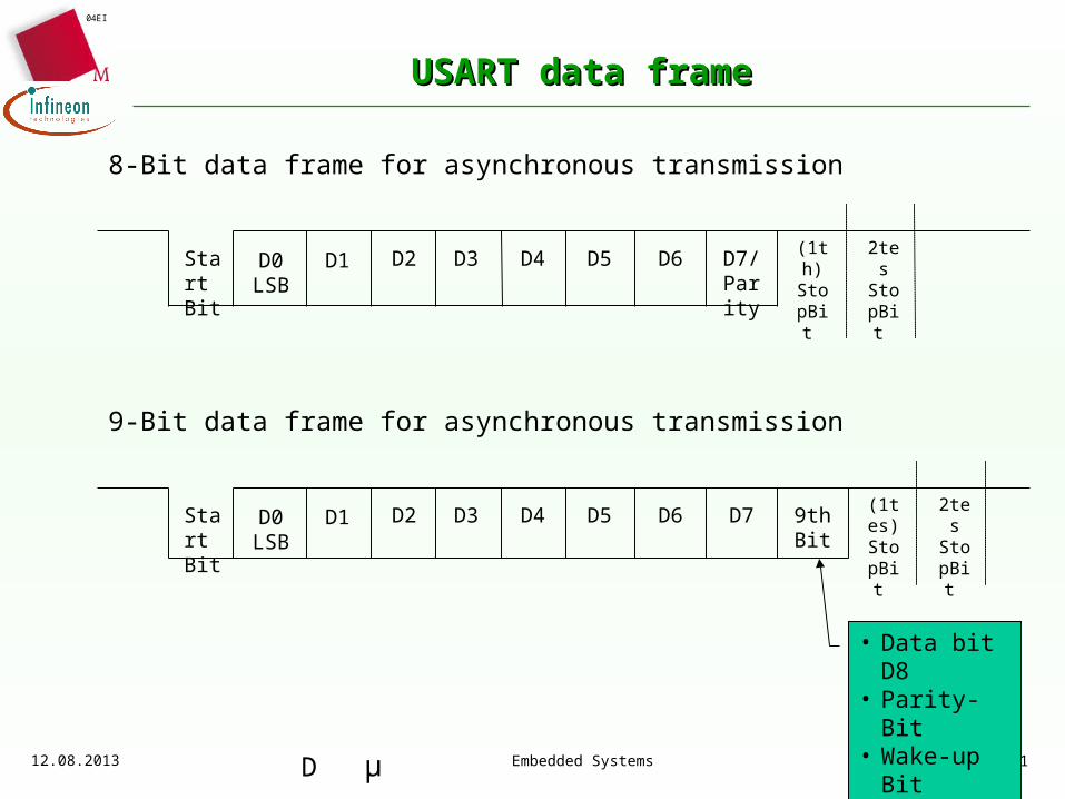
USART data frameUSART data frame
StartBit
D0LSB
D1
D2
D3
D4
D5
D6
D7/Parit
y
(1th)StopBit
2tesStopBit
8-Bit data frame for asynchronous transmission
StartBit
D0LSB
D1
D2
D3
D4
D5
D6
D7
9thBit
(1tes)StopBit
2tesStopBit
• Data bit D8• Parity-Bit• Wake-up Bit
9-Bit data frame for asynchronous transmission
µD
04EI
12.08.2013 Embedded Systems Page 12
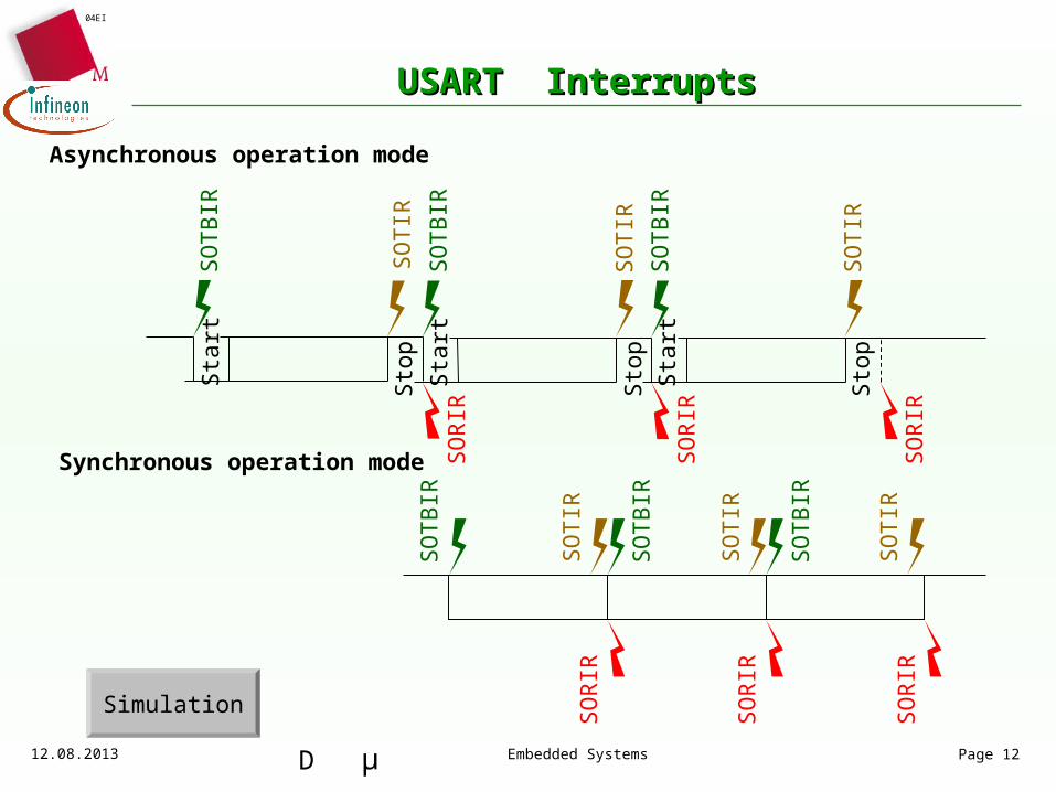
USART InterruptsUSART Interrupts
SO
TIR
SO
TIR
SO
TIR
SO
RIR
SO
RIR
SO
RIR
SO
TB
IR
SO
TB
IR
SO
TB
IR
Sta
rt
Sta
rt
Sta
rt
Sto
p
Sto
p
Sto
p
Asynchronous operation mode
SO
RIR
SO
RIR
SO
RIR
SO
TIR
SO
TIR
SO
TIR
SO
TB
IR
SO
TB
IR
SO
TB
IR
Synchronous operation mode
Simulation
µD
04EI
12.08.2013 Embedded Systems Page 13
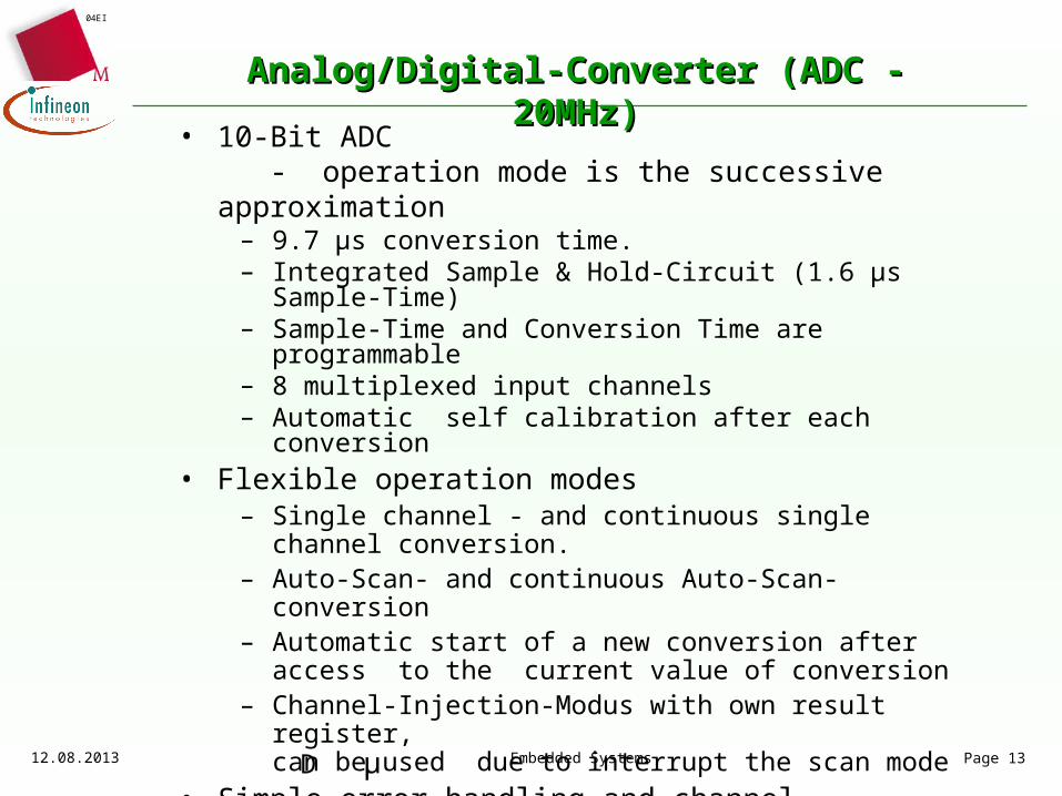
Analog/Digital-Converter (ADC - 20MHz)Analog/Digital-Converter (ADC - 20MHz)
• 10-Bit ADC - operation mode is the successive approximation
– 9.7 µs conversion time.– Integrated Sample & Hold-Circuit (1.6 µs Sample-Time)– Sample-Time and Conversion Time are programmable– 8 multiplexed input channels– Automatic self calibration after each conversion
• Flexible operation modes– Single channel - and continuous single channel conversion.– Auto-Scan- and continuous Auto-Scan-conversion– Automatic start of a new conversion after access to the
current value of conversion– Channel-Injection-Modus with own result register,
can be used due to interrupt the scan mode
• Simple error handling and channel identification– 10-Bit result is located together with the channel number in
the result register.– Test on Overrun error
µD
04EI
12.08.2013 Embedded Systems Page 14
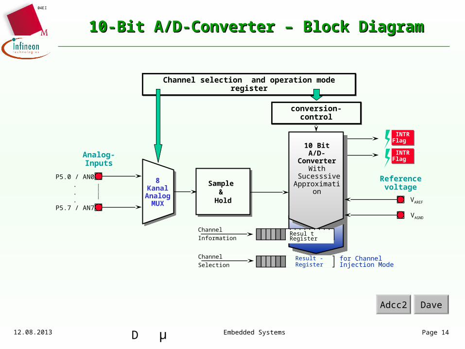
Analog-Inputs
Channel selection and operation mode registerChannel selection and operation mode register
Referencevoltage
8KanalAnalogMUX
Sample &
Hold
Sample &
Hold
INTR Flag INTR Flag
INTR Flag INTR Flag
10-Bit A/D-Converter – Block Diagram10-Bit A/D-Converter – Block Diagram
10 BitA/D-Converter
With Sucesssive
Approximation
Channel
Information
Channel
SelectionResult -Register
P5.0 / AN0...
P5.7 / AN7
Resul t Register
for Channel Injection Mode
VAREF
VAGND
conversion-controlconversion-control
Adcc2 Dave
µD
04EI
12.08.2013 Embedded Systems Page 15
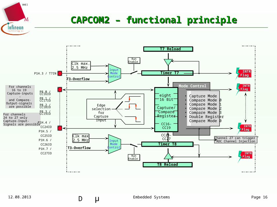
Capture / Compare Unit 2 (CAPCOM2-20 MHz) Capture / Compare Unit 2 (CAPCOM2-20 MHz)
• Two 16-Bit Timer (T7,T8), with 16-Bit Reload- Register for each Timer: Internal clock with prescaler up to 2.5 MHz (400ns).– Counter: External clock input at T7IN up to 1.25 MHz, the T3-
output signal (GPT1) can be used as clock input
• One registerfield with 16-Bit Capture/Compare Registers.– Individually programmable for the Capture- or one of the
Compare- modes– Individually assignable to the Timers T7 or T8
• Various Compare-modes for flexible generation Pulse-Width- Modulation (PWM) signals– Output-Pin changes its signal stage in case of positive
Compare.– 1 or 2 Compare-Registers act to one output-pin.– 1 or more Compare-events can be happen in one period of the
Timer – Operation modes, which are only cause interrupts, are possible
• Capture-Mode with selectable input edge.
µD
04EI
12.08.2013 Embedded Systems Page 16
CAPCOM2 – functional principleCAPCOM2 – functional principle
Edge selection for
Capture Input
InputMode
Control
T7 Reload T7 Reload
RunEnable
RunEnable
Clk max.2.5 MHzClk max.2.5 MHz
T8 Reload T8 Reload
Timer T8 Timer T8
Timer T7 Timer T7
Mode Control
INTRINTR Flag Flag INTRINTR Flag Flag
INTRINTR Flag Flag INTRINTR Flag Flag
INTRINTR Flag Flag INTRINTR Flag Flag
INTRINTR Flag Flag INTRINTR Flag Flag
T3-Overflow
InputMode
Control
Clk max2.5 MHzClk max2.5 MHz
For channels24 to 27 onlyCapture-Input-Signals are possible
Channel 27 can trigger “ADC Channel Injection”
• Capture Mode• Compare Mode 0• Compare Mode 1• Compare Mode 2• Compare Mode 3• Double Register Compare Mode 0
P1H.3 / T7IN
P8.0 / CC16IO
P8.1 / CC17IO
P8.2 / CC18IO
P8.3 / CC19IO
P1H.4 /
CC24IO
P1H.5 /
CC25IO
P1H.6 /
CC26IO
P1H.7 /
CC27IO
eight 16 Bit
Capture/CompareRegister
CC16-CC19
CC24-CC27
RunEnable
RunEnable
For channels16 to 19
Capture-inputs -and Compare-Output-signals
are possible
T3-Overflow
µD
04EI
12.08.2013 Embedded Systems Page 17
Mode 0: Only the INTR Flags are set
Mode 1:The INTR Flags are set, the state of the Port-Pin is inverted
Com
pare
IN
TR
Ti m
erIN
TR
Com
pare
IN
TR
Port LevelP8.x
CAPCOM2: Compare ModesCAPCOM2: Compare Modes
• Modus 0 and1: Several Compare-events per timer period are possible
New
Reload Value
Compare Value 2
Compare Value 1
FFFF
Reload value
Value 1 Value 2
is changed to
Compare Register X:
• Mode 2 and 3: Only one Compare-event per timer-period is generatedMode 2:
Only the INTR Flags are set
Mode 3:die INTR Flags are set, the state of the Port-Pin is set at a compare event and is reset at Timer-Overrun
Com
pare
IN
TR
Tim
er I
NT
R
Port Level P8.x
FFFF
Compare Value 2
Compare Value 1Reload Value
New
Reload Value
is changed toValue 1 Value 2Compare Register X:
µD
04EI
12.08.2013 Embedded Systems Page 18
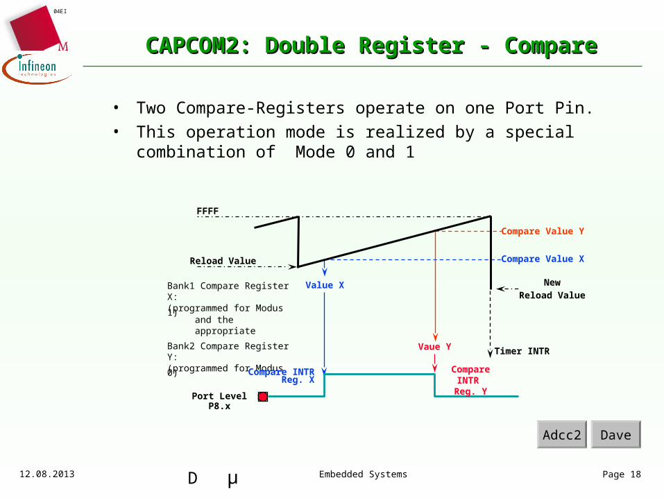
CAPCOM2: Double Register - CompareCAPCOM2: Double Register - Compare
• Two Compare-Registers operate on one Port Pin.
• This operation mode is realized by a special combination of Mode 0 and 1
Vaue Y
Compare Value Y
Compare Value X
FFFF
Reload Value
New
Reload ValueValue XBank1 Compare Register X:
(programmed for Modus 1)
and the appropriate
Bank2 Compare Register Y:(programmed for Modus 0)
Timer INTR
Port Level P8.x
Compare INTR
Reg. Y
Compare INTRReg. X
Adcc2 Dave
µD
04EI
12.08.2013 Embedded Systems Page 19
164CL
XTAL
C166-CoreC166-Core
Port 5 Port 3
CPU
Dua
l Por
t
RAM
2 KByte
Interrupt Controller
Watchdog
Peripheral Data
External Instr./Data
Instr./Data
USART
ASC
BRG
GPT1
16
16
16
1632
PEC
64 K ROM
(C164 CI-8RM)or
OTP(C164CI-8EM)
Interrupt Bus
Data
Data
Port 8
BRG
SSC
Sync. Channel(SPI)
PLL-Oscillatorprog. Multiplier:
0.5; 1; 1.5; 2;2.5; 3; 4; 5
XB
US
(16-
bit N
ON
MU
X D
ata
/ Add
ress
es)
T2
T4
T3
13 ext. IR
Full-CANInterfaceV2.0Bactive
RTC
10-BitADC
Tim
er 7
Tim
er 8
Port 1
Tim
er 1
3
1 Comp.Channel
3/6 CAPCOMChannels
CAPCOM6 Unit forPWM Generation
8 9 4 16
6
16
Port 4
8-Channels
External Bus8/16 bit
MUX only&
XBUSControl
CAPCOM 2
8-Channel
C164CI – clock distribution
P4.6/ CAN TxD
P4.5/ CANRxD
Port
0
µD
04EI
1208.2013 Embedded Systems Page 20
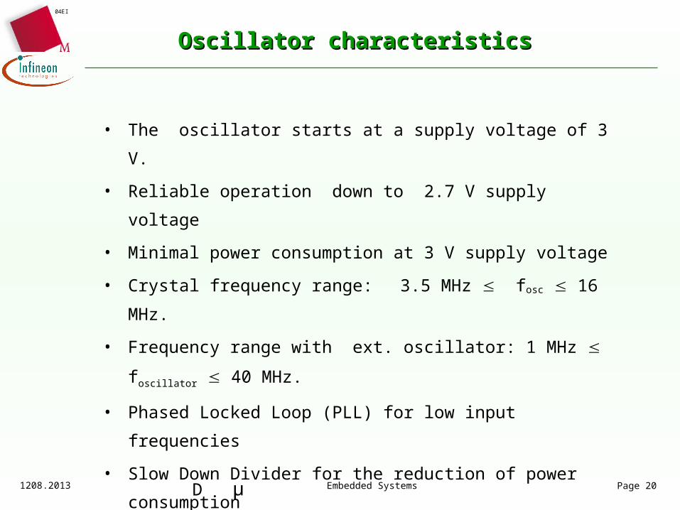
Oscillator characteristicsOscillator characteristics
• The oscillator starts at a supply voltage of 3 V.
• Reliable operation down to 2.7 V supply voltage
• Minimal power consumption at 3 V supply voltage
• Crystal frequency range: 3.5 MHz fosc 16 MHz.
• Frequency range with ext. oscillator: 1 MHz foscillator 40 MHz.
• Phased Locked Loop (PLL) for low input frequencies
• Slow Down Divider for the reduction of power consumption
• Separate clock driver for different ranges of the system
µD
04EI
27.9.2009 Embedded Systems Page 21
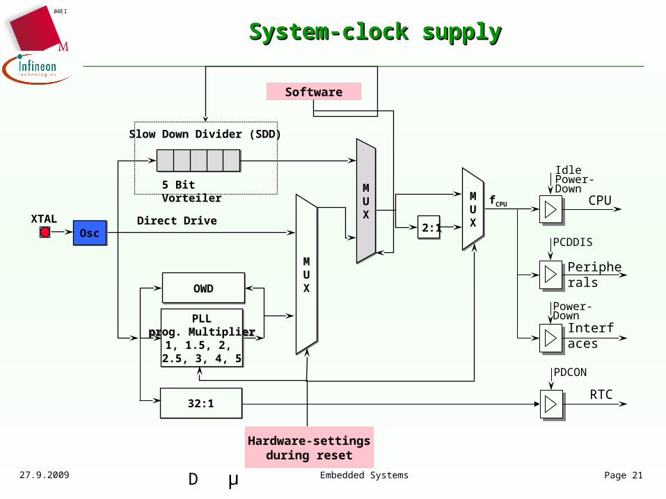
System-clock supplySystem-clock supply
Software
Slow Down Divider (SDD)
2:1 2:1
fCPU
PLLprog. Multiplier
1, 1.5, 2, 2.5, 3, 4, 5
PLLprog. Multiplier
1, 1.5, 2, 2.5, 3, 4, 5
OWDOWD
MUX
MUX
Hardware-settings during reset
MUX
MUX
Direct Drive
MUX
MUX
OscOscXTAL
5 Bit Vorteiler
32:132:1RTC
Interfaces
Peripherals
CPU
IdlePower-Down
PCDDIS
Power-Down
PDCON
µD
04EI
12.08.2013 Embedded Systems Page 22
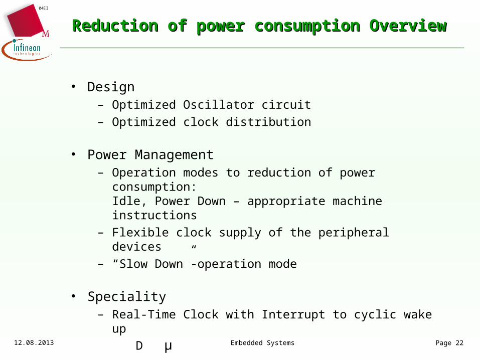
Reduction of power consumption OverviewReduction of power consumption Overview
• Design– Optimized Oscillator circuit
– Optimized clock distribution
• Power Management– Operation modes to reduction of power consumption:
Idle, Power Down – appropriate machine instructions
– Flexible clock supply of the peripheral devices
– “Slow Down”-operation mode
• Speciality– Real-Time Clock with Interrupt to cyclic wake up
µD
04EI
12.08.2013 Embedded Systems Page 23
Power ManagementPower Management
RTCRTC
PLLPLL
EXIN
ASC
SSCCLK
EN
fCPU
fPeripherieSlow Down DeviderSlow Down Devider
System Clock Generation Peripherals
ADC
GPT1
CAPCOM2
CAN
InterruptController
CLK WDT
CAPCOM6
CLK Clock DriverRTC
Power Down
CLK InterfaceClock Driver
Clock DriverCPU
OscillatorOscillatorXTAL
CLK
CLKEN
CLK
EN
CLK
EN
CLK
EN
CLK
EN
CLK
EN
CLK
PeripheralClock Driver
CLK
EN
CLK
EN
fSystem
fRTC
Interface Peripherals
Idle Mode
µD
04EI
12.08.2013 Embedded Systems Page 24
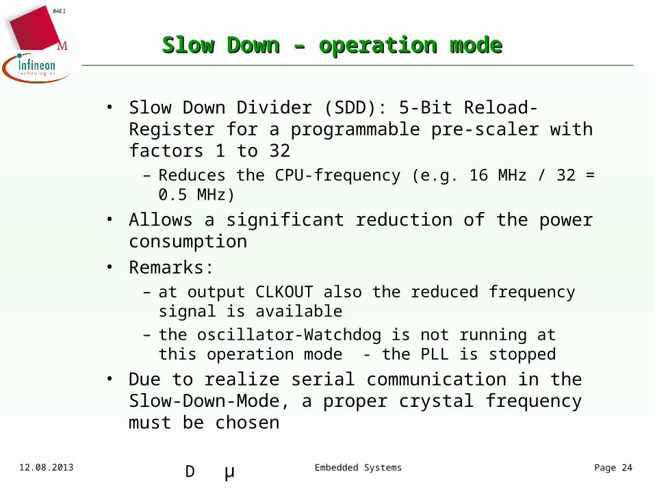
Slow Down – operation mode Slow Down – operation mode
• Slow Down Divider (SDD): 5-Bit Reload-Register for a programmable pre-scaler with factors 1 to 32
– Reduces the CPU-frequency (e.g. 16 MHz / 32 = 0.5 MHz)
• Allows a significant reduction of the power consumption• Remarks:
– at output CLKOUT also the reduced frequency signal is available
– the oscillator-Watchdog is not running at this operation mode - the PLL is stopped
• Due to realize serial communication in the Slow-Down-Mode, a proper crystal frequency must be chosen
µD
04EI
12.08.2013 Embedded Systems Page 25
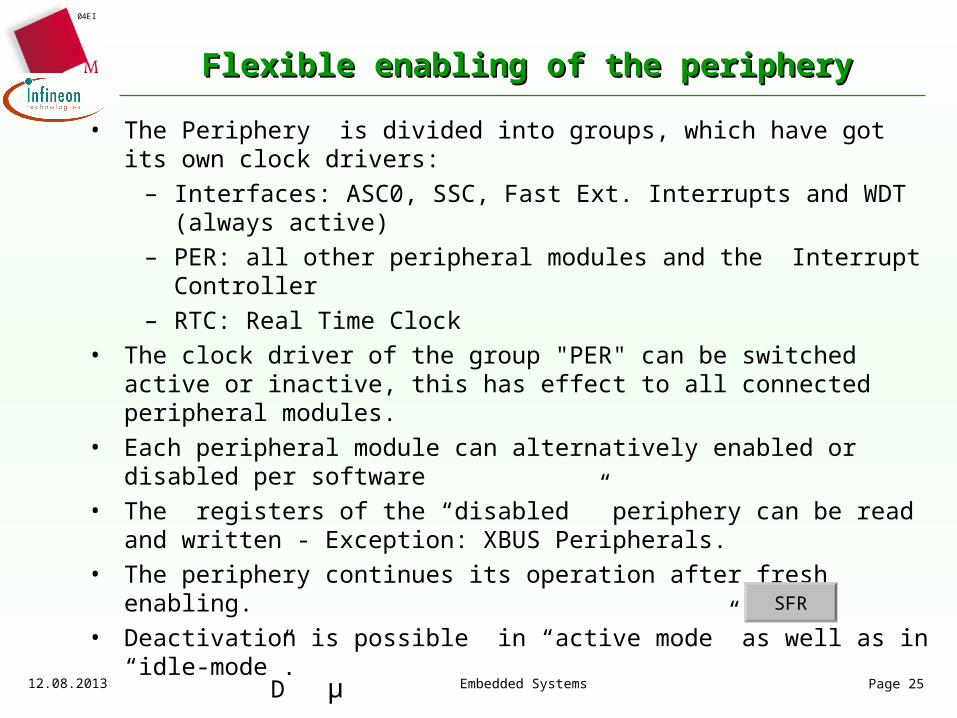
Flexible enabling of the peripheryFlexible enabling of the periphery
• The Periphery is divided into groups, which have got its own clock drivers:
– Interfaces: ASC0, SSC, Fast Ext. Interrupts and WDT (always active)
– PER: all other peripheral modules and the Interrupt Controller
– RTC: Real Time Clock
• The clock driver of the group "PER" can be switched active or inactive, this has effect to all connected peripheral modules.
• Each peripheral module can alternatively enabled or disabled per software
• The registers of the “disabled ” periphery can be read and written - Exception: XBUS Peripherals.
• The periphery continues its operation after fresh enabling.
• Deactivation is possible in “active mode” as well as in “idle-mode”.
SFR
µD
04EI
12.08.2013 Embedded Systems Page 26
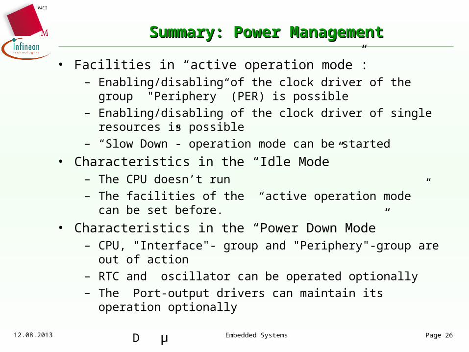
Summary: Power ManagementSummary: Power Management
• Facilities in “active operation mode”:– Enabling/disabling of the clock driver of the group "Periphery”
(PER) is possible
– Enabling/disabling of the clock driver of single resources is possible
– “Slow Down”- operation mode can be started
• Characteristics in the “Idle Mode”– The CPU doesn’t run
– The facilities of the “active operation mode ” can be set before.
• Characteristics in the “Power Down Mode”– CPU, "Interface"- group and "Periphery"-group are out of action
– RTC and oscillator can be operated optionally
– The Port-output drivers can maintain its operation optionally

µD
04EI
12.08.2013 Embedded Systems Page 27
Power Consumption
Active Mode
Idle Mode
Power Down Mode Ports: OFF RTC / OSC: OFF
Power Down Mode Ports: ON RTC / OSC: OFF
Power Down Mode Ports: OFF RTC / OSC: ON
Power Down Mode Ports: ON RTC / OSC: ON
Active Mode and disabled "PER" group clock driver
Idle Mode and disabled "PER" group clock driver
Flexible Peripheral Management
Flexible Peripheral Management
Active or Idle Mode
Active or Idle Mode
SLOW
DOWN
Power Consumption
Overview of the estimated power consumptionOverview of the estimated power consumption
µD
04EI
27.9.2009 Embedded Systems Page 28
164CL
XTAL
C166-CoreC166-Core
Port 5 Port 3
CPU
Dua
l Por
t
RAM
2 KByte
Interrupt Controller
Watchdog
Peripheral Data
External Instr./Data
Instr./Data
USART
ASC
BRG
GPT1
16
16
16
1632
PEC
64 K ROM
(C164 CI-8RM)or
OTP(C164CI-8EM)
Interrupt Bus
Data
Data
Port 8
BRG
SSC
Sync. Channel(SPI)
PLL-Oscillatorprog. Multiplier:
0.5; 1; 1.5; 2;2.5; 3; 4; 5
XB
US
(16-
bit N
ON
MU
X D
ata
/ Add
ress
es)
T2
T4
T3
13 ext. IR
Full-CANInterfaceV2.0Bactive
RTC
10-BitADC
Tim
er 7
Tim
er 8
Port 1
Tim
er 1
3
1 Comp.Channel
3/6 CAPCOMChannels
CAPCOM6 Unit forPWM Generation
8 9 4 16
6
16
Port 4
8-Channels
External Bus8/16 bit
MUX only&
XBUSControl
CAPCOM 2
8-Channel
C164CI - The PeripheryC164CI - The Periphery
P4.6/ CAN TxD
P4.5/ CANRxD
Port
0

µD
04EI
12.08.2013 Embedded Systems Page 29
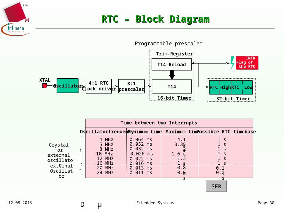
Real-Time Clock (RTC)Real-Time Clock (RTC)
• Is countering Time Ticks
• The ticks are – independent from the CPU-clock- determined, by the external crystal frequency and a programmable prescaler
• Cyclic time based InterruptThe cycle time can be determined via a reload register
• Additional function
The RTC-Register (32 Bit) and the programmable pre-scaler can be cascaded to a 48-Bit time base
µD
04EI
12.08.2013 Embedded Systems Page 30
Crystal orexternal oscillator
Time between two Interrupts
Oscillatorfrequency Minimum time Maximum time Possible RTC-timebase
1 s4 MHz 0.064 ms 4.1 s5 MHz 0.052 ms 3.35 s 1 s8 MHz 0.032 ms 2 s 1 s
10 MHz 0.026 ms 1.6 s 1 s12 MHz 0.022 ms 1.3 s 1 s16 MHz 0.016 ms 1 s 1 s20 MHz 0.013 ms 0.8 s 0.1 s24 MHz 0.011 ms 0.6 s 0.1 s
external Oscillator
RTC – Block DiagramRTC – Block Diagram
4:1 RTCClock driver
4:1 RTCClock driver
8:1prescaler
8:1prescaler
OscillatorOscillatorXTAL
T14T14
16-bit Timer
T14-ReloadT14-Reload
Trim-Register
Programmable prescaler
INTRFlag of
the RTC
INTRFlag of
the RTC
RTC Low RTC High
32-bit Timer
SFR
µD
04EI
12.08.2013 Embedded Systems Page 31
RTC-based cyclic interruptRTC-based cyclic interrupt
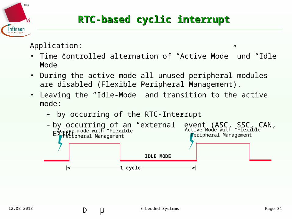
Application:
• Time controlled alternation of “Active Mode” und “Idle Mode”
• During the active mode all unused peripheral modules are disabled (Flexible Peripheral Management).
• Leaving the “Idle-Mode” and transition to the active mode:
– by occurring of the RTC-Interrupt
– by occurring of an “external” event (ASC, SSC, CAN, EXIN).
IDLE MODE
1 cycle
Active mode with “FlexiblePeripheral Management”
Active Mode with “FlexiblePeripheral Management”
µD
04EI
27.9.2009 Embedded Systems Page 32
Watchdog Timer (WDT) - 20 MHzWatchdog Timer (WDT) - 20 MHz
• Overrun of a 16-Bit-couter results in:– System Reset
– Activating of the output signal RSTOUT
– Set of the corresponding control bit
– WDT is still active
• Programmable input clock derived from system clock• 8-Bit-reload register for the higher significant Byte• Counter period n from 25.6µs to 470ms• Reset of the counter register (Reload) is done via special
instruction
µD
04EI
12.08.2013 Embedded Systems Page 33
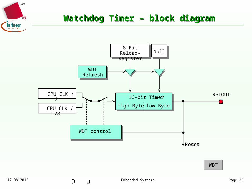
WDTRefresh
8-BitReload-Register Null
RSTOUT
Reset
16-bit Timer
high Byte low Byte
WDT control
CPU CLK / 2
Watchdog Timer – block diagramWatchdog Timer – block diagram
CPU CLK / 128
WDT
µD
04EI
12.08.2013 Embedded Systems Page 34
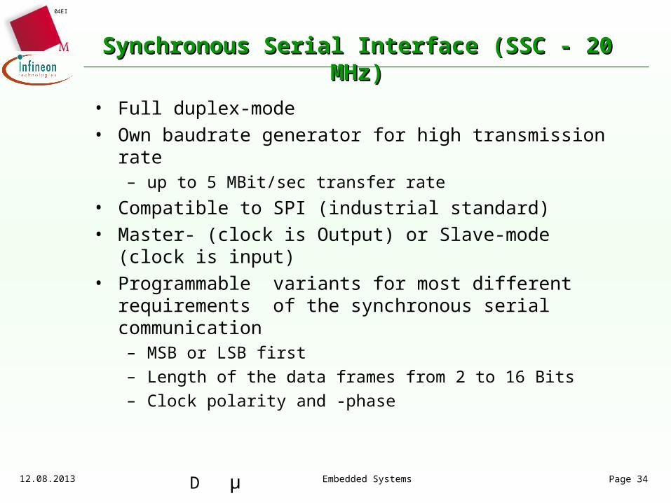
Synchronous Serial Interface (SSC - 20 MHz)Synchronous Serial Interface (SSC - 20 MHz)
• Full duplex-mode• Own baudrate generator for high transmission rate
– up to 5 MBit/sec transfer rate
• Compatible to SPI (industrial standard)• Master- (clock is Output) or Slave-mode (clock is input)• Programmable variants for most different requirements of
the synchronous serial communication– MSB or LSB first
– Length of the data frames from 2 to 16 Bits
– Clock polarity and -phase
µD
04EI
12.08.2013 Embedded Systems Page 35
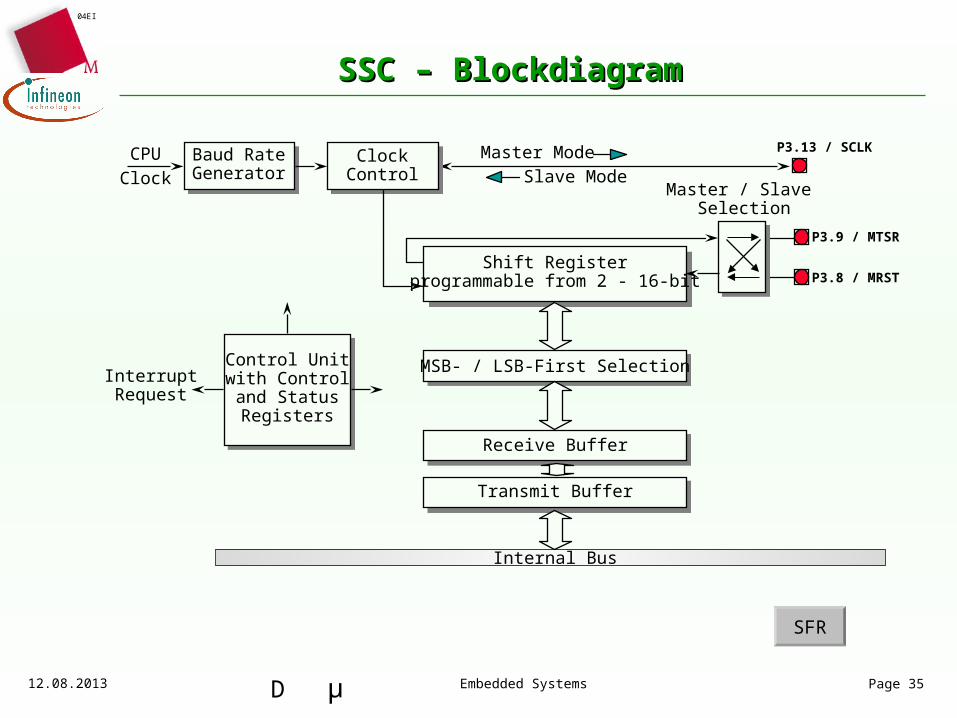
SSC – BlockdiagramSSC – Blockdiagram
Baud RateGenerator
ClockControl
Control Unitwith Controland StatusRegisters
Shift Registerprogrammable from 2 - 16-bit
MSB- / LSB-First Selection
Receive Buffer
Transmit Buffer
Internal Bus
InterruptRequest
Slave Mode
Master ModeCPU
ClockMaster / Slave
Selection
P3.13 / SCLK
P3.8 / MRST
P3.9 / MTSR
SFR
µD
04EI
12.08.2013 Embedded Systems Page 36
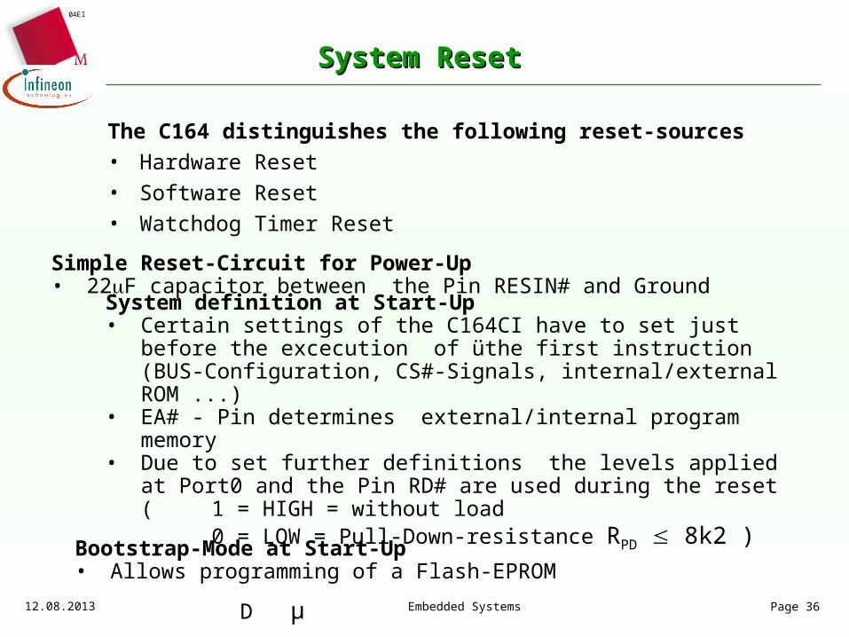
System ResetSystem Reset
The C164 distinguishes the following reset-sources
• Hardware Reset
• Software Reset
• Watchdog Timer Reset
Simple Reset-Circuit for Power-Up• 22F capacitor between the Pin RESIN# and Ground
System definition at Start-Up• Certain settings of the C164CI have to set just before the excecution of
üthe first instruction (BUS-Configuration, CS#-Signals, internal/external ROM ...)
• EA# - Pin determines external/internal program memory• Due to set further definitions the levels applied at Port0 and the Pin
RD# are used during the reset ( 1 = HIGH = without load
0 = LOW = Pull-Down-resistance RPD 8k2 )
Bootstrap-Mode at Start-Up• Allows programming of a Flash-EPROM
µD
04EI
12.08.2013 Embedded Systems Page 37
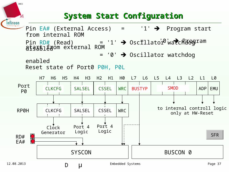
System Start ConfigurationSystem Start Configuration
Pin EA# (External Access) = '1' Program start from internal ROM = '0' Program start from external ROMPin RD# (Read) = '1' Oscillator watchdog disabled
= ‘0' Oscillator watchdog enabled
SFR
Reset state of Port0 P0H, P0L
H7 H6 H5 H4 H3 H2 H1 H0 L7 L6 L5 L4 L3 L2 L1 L0
Port P0 SALSEL CSSEL WRC BUSTYP ADP EMU
CLKCFG SALSEL CSSEL WRCRP0H
ClockGenerator
Port 4Logic
Port 4Logic
to internal controll logiconly at HW-Reset
SYSCON BUSCON 0
CLKCFG
RD#
SMOD
EA#
µD
04EI
12.08.2013 Embedded Systems Page 38
Bootstrap LoaderBootstrap Loader
• SMOD = 1011 during a Hardware-Reset
• ASC0 is waiting for a Null-Byte
• From the duration of the Null-Bytes automatically the necessary baudrate is detected
• C164 returns an identifier with this baudrate
• Exactly 32 Bytes are deposited via the serial interface in the internal RAM at 0xFA40 - 0xFA5F
• Afterward the program start at address 0xFA40 is executed
CodeExample


![The modern port of patras el[1]](https://static.fdocument.org/doc/165x107/557ea112d8b42ac5658b47de/the-modern-port-of-patras-el1.jpg)