ΗΜΥ 664 ΨΗΦΙΑΚΟΣ ΣΧΕΔΙΑΣΜΟΣ ΜΕ FPGAs 2010 … · At logic design or...
71
ΗΜ648 L6 Design and Reuse of Components.1 © Θεοχαρίδης, ΗΜΥ, 2010 ΗΜΥ 664 ΨΗΦΙΑΚΟΣ ΣΧΕΔΙΑΣΜΟΣ ΜΕ FPGAs Χειμερινό Εξάμηνο 2010 ΔΙΑΛΕΞΗ 6: Design and Reuse of Components ΧΑΡΗΣ ΘΕΟΧΑΡΙΔΗΣ ([email protected])
Transcript of ΗΜΥ 664 ΨΗΦΙΑΚΟΣ ΣΧΕΔΙΑΣΜΟΣ ΜΕ FPGAs 2010 … · At logic design or...
ΗΜ648 L6 Design and Reuse of Components.1 © Θεοχαρίδης, ΗΜΥ, 2010
ΗΜΥ 664ΨΗΦΙΑΚΟΣ ΣΧΕΔΙΑΣΜΟΣ ΜΕ FPGAsΧειμερινό Εξάμηνο 2010
ΔΙΑΛΕΞΗ 6:Design and Reuse of Components
ΧΑΡΗΣ ΘΕΟΧΑΡΙΔΗΣ([email protected])
Presenter
Presentation Notes
Other handouts To handout next time
ΗΜ648 L6 Design and Reuse of Components.2 © Θεοχαρίδης, ΗΜΥ, 2010
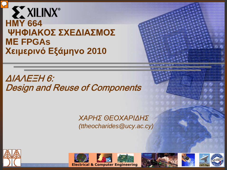
Design Process Steps (Review)
Definition of system requirements. Example: ISA (instruction set architecture) for CPU. Includes software and hardware interfaces including
timing. May also include cost, speed, reliability and
maintainability specifications.
Definition of system architecture. Example: high-level HDL (hardware description
language) representation - this is not required in ECE664 but is done in the real world).
Useful for system validation and verification and as a basis for lower level design execution and validation or verification.
ΗΜ648 L6 Design and Reuse of Components.3 © Θεοχαρίδης, ΗΜΥ, 2010
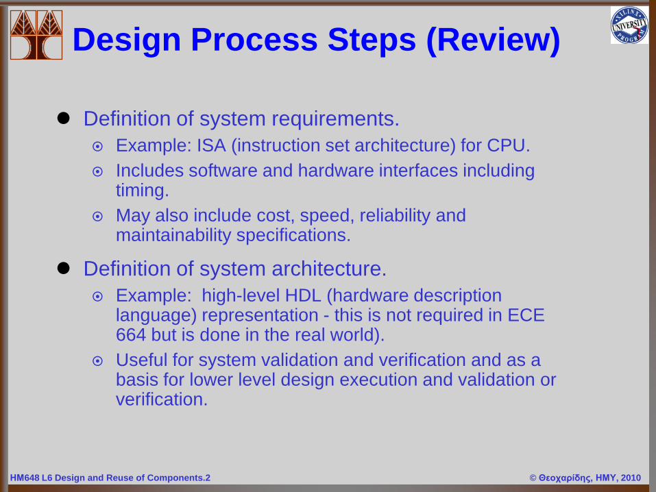
Design Process Steps (Review)
Refinement of system architecture In manual design, descent in hierarchy, designing
increasingly lower-level components In synthesized design, transformation of high-level HDL to
“synthesizable” register transfer level (RTL) HDL
Logic design or synthesis In manual or synthesized design, development of logic
design in terms of library components Result is logic level schematic or netlist representation or
combinations of both. Both manual design or synthesis typically involve
optimization of cost, area, or delay.
ΗΜ648 L6 Design and Reuse of Components.4 © Θεοχαρίδης, ΗΜΥ, 2010
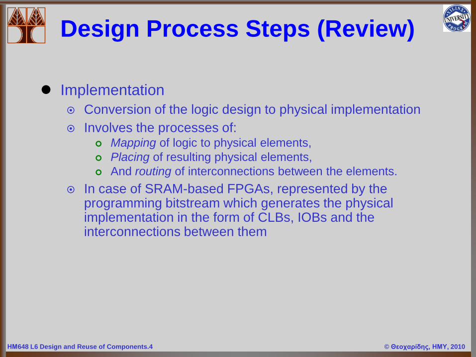
Design Process Steps (Review)
Implementation Conversion of the logic design to physical implementation Involves the processes of:
Mapping of logic to physical elements, Placing of resulting physical elements, And routing of interconnections between the elements.
In case of SRAM-based FPGAs, represented by the programming bitstream which generates the physical implementation in the form of CLBs, IOBs and the interconnections between them
ΗΜ648 L6 Design and Reuse of Components.5 © Θεοχαρίδης, ΗΜΥ, 2010
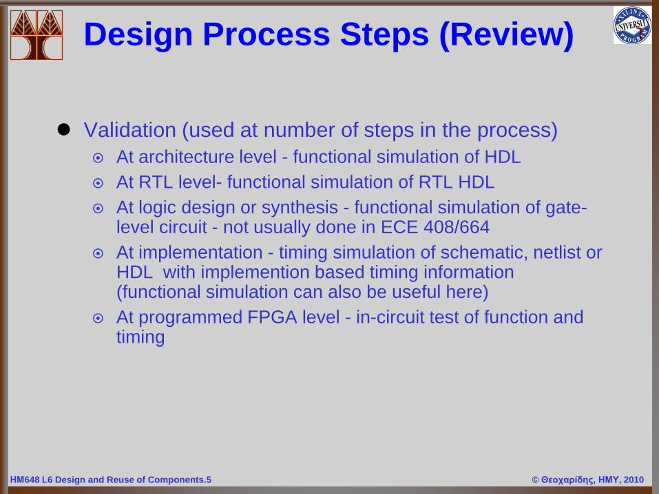
Design Process Steps (Review)
Validation (used at number of steps in the process) At architecture level - functional simulation of HDL At RTL level- functional simulation of RTL HDL At logic design or synthesis - functional simulation of gate-
level circuit - not usually done in ECE 408/664 At implementation - timing simulation of schematic, netlist or
HDL with implemention based timing information (functional simulation can also be useful here)
At programmed FPGA level - in-circuit test of function and timing
ΗΜ648 L6 Design and Reuse of Components.6 © Θεοχαρίδης, ΗΜΥ, 2010
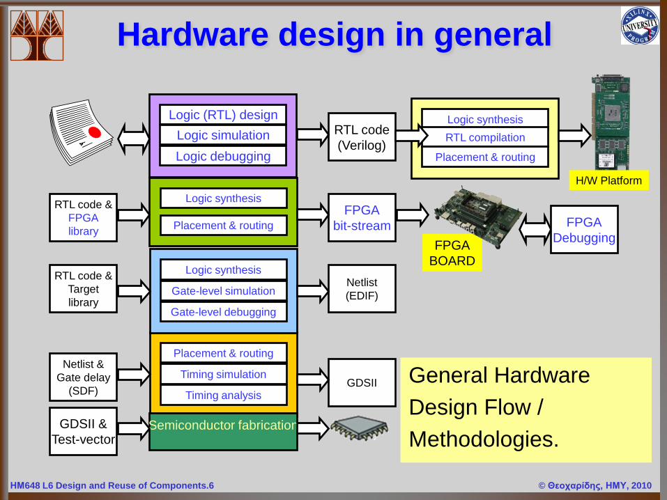
Hardware design in general
Logic (RTL) designLogic simulationLogic debugging
RTL code(Verilog)
Placement & routing
Timing simulation
Timing analysis
Netlist &Gate delay
(SDF)GDSII
Semiconductor fabricationGDSII &Test-vector
Logic synthesis
Gate-level simulation
Gate-level debugging
Netlist(EDIF)
RTL code &Targetlibrary
Logic synthesis
Placement & routingFPGA
bit-stream
RTL code &FPGAlibrary
FPGABOARD
FPGADebugging
Logic synthesisRTL compilation
Placement & routing
H/W Platform
General HardwareDesign Flow /Methodologies.
ΗΜ648 L6 Design and Reuse of Components.7 © Θεοχαρίδης, ΗΜΥ, 2010
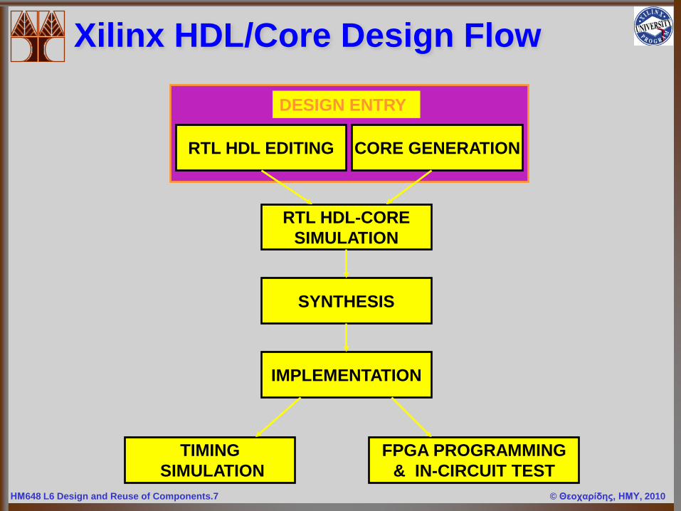
Xilinx HDL/Core Design Flow
DESIGN ENTRY
CORE GENERATIONRTL HDL EDITING
RTL HDL-CORESIMULATION
SYNTHESIS
IMPLEMENTATION
TIMINGSIMULATION
FPGA PROGRAMMING& IN-CIRCUIT TEST
ΗΜ648 L6 Design and Reuse of Components.8 © Θεοχαρίδης, ΗΜΥ, 2010
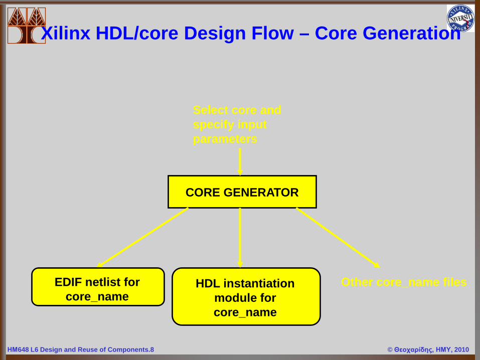
Xilinx HDL/core Design Flow – Core Generation
CORE GENERATOR
Select core and specify input parameters
HDL instantiation module for core_name
EDIF netlist for core_name
Other core_name files
ΗΜ648 L6 Design and Reuse of Components.9 © Θεοχαρίδης, ΗΜΥ, 2010
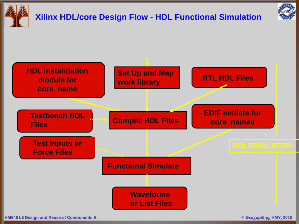
Xilinx HDL/core Design Flow - HDL Functional Simulation
Compile HDL Files
Waveforms or List Files
Set Up and Map work library RTL HDL Files
Test Inputs or Force Files
HDL instantiation module for core_name
EDIF netlists for core_names
Functional Simulate
Testbench HDL Files
HDLSIMULATOR
ΗΜ648 L6 Design and Reuse of Components.10 © Θεοχαρίδης, ΗΜΥ, 2010
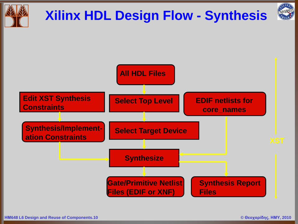
All HDL Files
Gate/Primitive Netlist Files (EDIF or XNF)
Xilinx HDL Design Flow - Synthesis
Select Top Level
Select Target Device
Edit XST Synthesis Constraints
Synthesize
Synthesis/Implement-ation Constraints
Synthesis Report Files
EDIF netlists for core_names
XST
ΗΜ648 L6 Design and Reuse of Components.11 © Θεοχαρίδης, ΗΜΥ, 2010
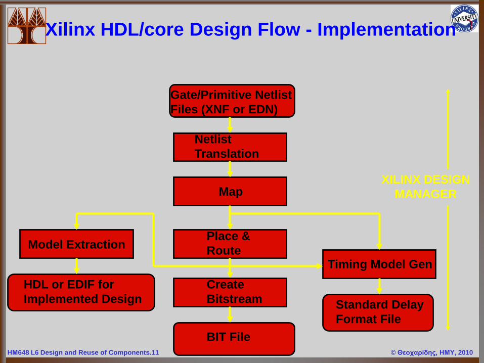
Model Extraction
Xilinx HDL/core Design Flow - Implementation
Netlist Translation
Map
Place & Route
BIT File
Create Bitstream
Timing Model Gen
Gate/Primitive Netlist Files (XNF or EDN)
Standard Delay Format File
HDL or EDIF for Implemented Design
XILINX DESIGN MANAGER
ΗΜ648 L6 Design and Reuse of Components.12 © Θεοχαρίδης, ΗΜΥ, 2010
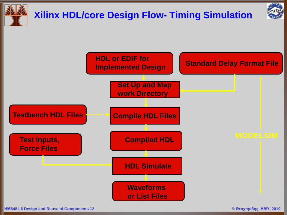
Xilinx HDL/core Design Flow- Timing Simulation
Test Inputs, Force Files
MODELSIM
Compile HDL Files
Waveforms or List Files
Set Up and Map work Directory
Compiled HDL
HDL Simulate
Standard Delay Format FileHDL or EDIF for Implemented Design
Testbench HDL Files
ΗΜ648 L6 Design and Reuse of Components.13 © Θεοχαρίδης, ΗΜΥ, 2010
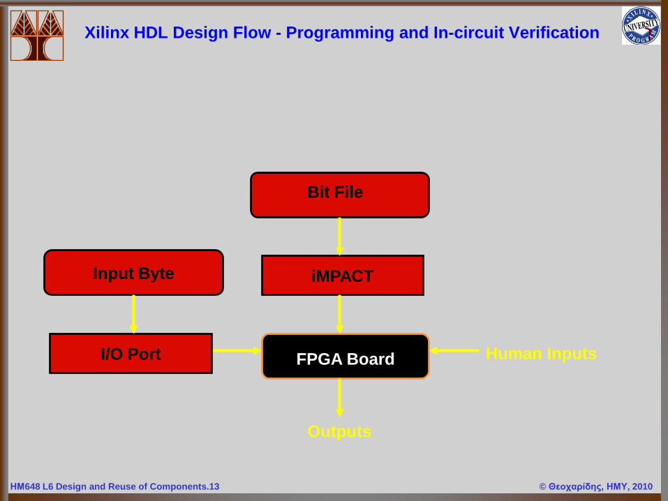
Xilinx HDL Design Flow - Programming and In-circuit Verification
Bit File
FPGA Board
iMPACT
I/O Port
Input Byte
Human Inputs
Outputs
ΗΜ648 L6 Design and Reuse of Components.14 © Θεοχαρίδης, ΗΜΥ, 2010
The Xilinx Libraries
Useful only if you have to instantiate (in your HDL) Xilinx primitives or macros (not all can be instantiated) from the Libraries guide.
Note selection guide includes CLB counts and section at front on notation used to describe macros.

ΗΜ648 L6 Design and Reuse of Components.15 © Θεοχαρίδης, ΗΜΥ, 2010
Design Practices Use synchronous design.
CLBs are actually reading functions from SRAM! Avoid clock gating. Avoid ripple counters. Avoid use of direct sets and resets except for
initialization. Synchronize asynchronous signals as needed. Study timing issues handout.
ΗΜ648 L6 Design and Reuse of Components.16 © Θεοχαρίδης, ΗΜΥ, 2010
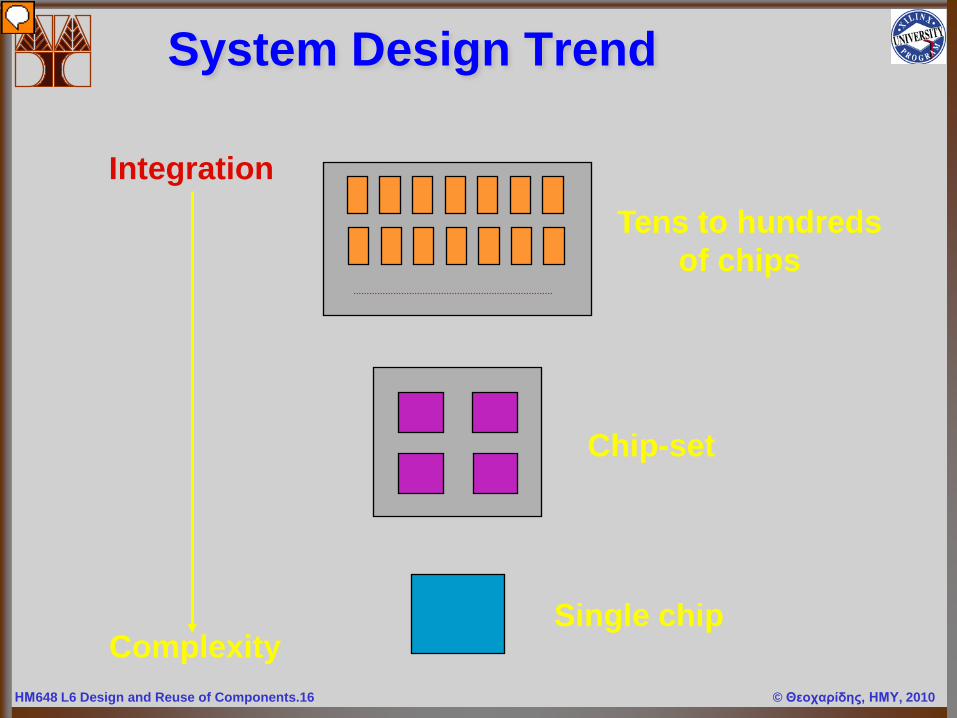
System Design Trend
Tens to hundredsof chips
Chip-set
Single chip
Integration
Complexity
Presenter
Presentation Notes
Due to the rapid progress on fab technology, system designs has evolved from several pcb consisting of tens-hundreds of chips, to a single pcb with chip sets, and today’s single chip (SOC).
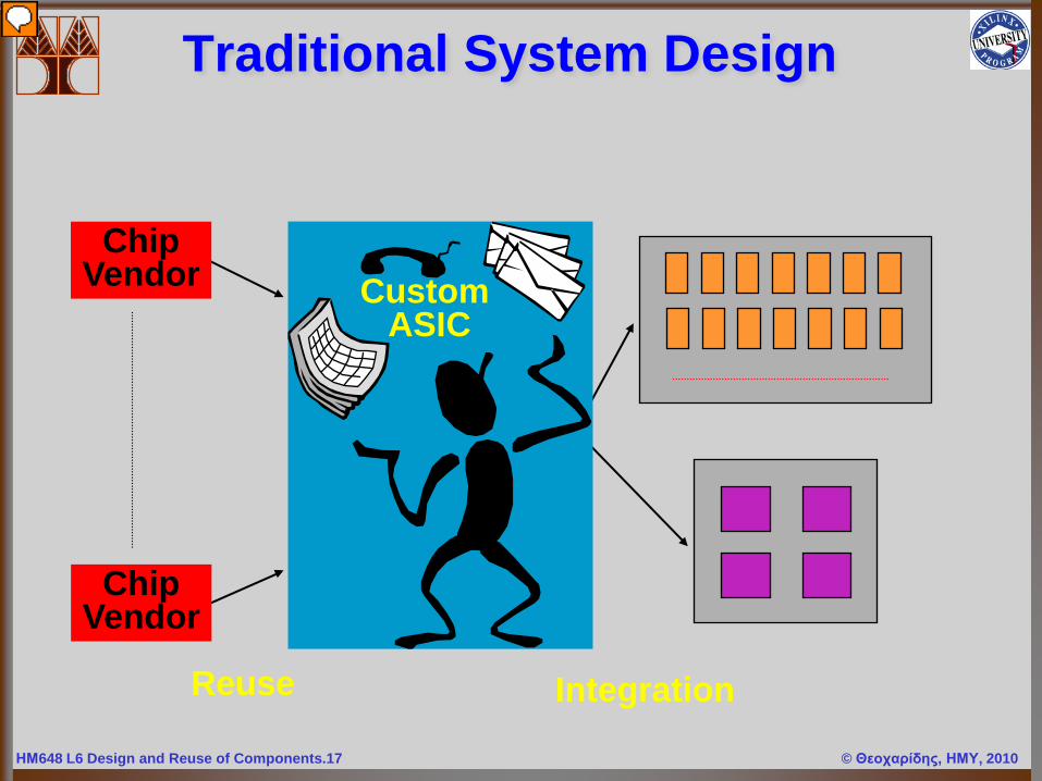
ΗΜ648 L6 Design and Reuse of Components.17 © Θεοχαρίδης, ΗΜΥ, 2010
Traditional System Design
ChipVendor
ChipVendor
Custom ASIC
Reuse Integration
Presenter
Presentation Notes
In traditional system design process, designers first search the available chips and chip-sets from a variety of vendors. They then determine which chips/chip-sets or any custom ASICs they will use to implement their system design. Finally, they will integrate the chips/chip-set to realize their system design.
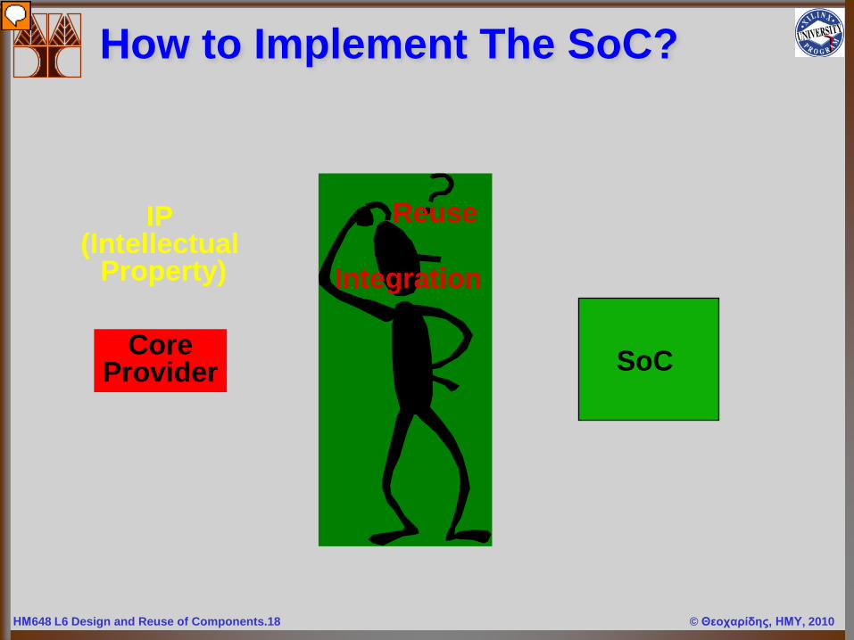
ΗΜ648 L6 Design and Reuse of Components.18 © Θεοχαρίδης, ΗΜΥ, 2010
How to Implement The SoC?
SoCCoreProvider
IP(Intellectual
Property)
Reuse
Integration
Presenter
Presentation Notes
Now, designers are trying to figure out how to develop their system using the SOC technology. For SOC designs, designers don’t have to search the available chips/chip-sets instead they have to search the available cores/IPs from core/IP vendors to implement their system.How to reuse and integrate cores/IPs are the two main problems confronting by all the SOC designers.
ΗΜ648 L6 Design and Reuse of Components.19 © Θεοχαρίδης, ΗΜΥ, 2010
Design Technology Status
Problems* Productivity gap* Shorter time-to-market* Designer shortage
Solutions* Higher levels of abstraction* New reuse methodology* New business model
Presenter
Presentation Notes
To enter SOC era, today’s design technology has the following three main problems: 1. Design productivity crisis, 2. Short time-to-market, 3. Designer shortage. The solutions to resolve the above three problems are: 1. Move the design abstraction to a higher level, 2. Design methodology for core/IP reuse, 3. New business model to couple core/IP reuse.
ΗΜ648 L6 Design and Reuse of Components.20 © Θεοχαρίδης, ΗΜΥ, 2010
Why Do We Need Reuse?
Reuse practice is everywhere
It has been a common practice in software developments for years.
It has been a common practice in electronic product developments for years.
=> Goal: makes our life easier!!!
Presenter
Presentation Notes
In this slide, we address what is reuse. Actually, reuse practice is everywhere in our daily life. For example, you want to eat salad and you like Italian dressing. Most likely you will go to a super-market to buy the dressing but not make your dressing start from scratch. This is a reuse practice “reuse the pre-made salad dressing”. We have practiced reuse method in our daily life over thousand years. Similarly, we have applied the reuse practice to software development and electronic-product designs. The goal is to make our life easier.
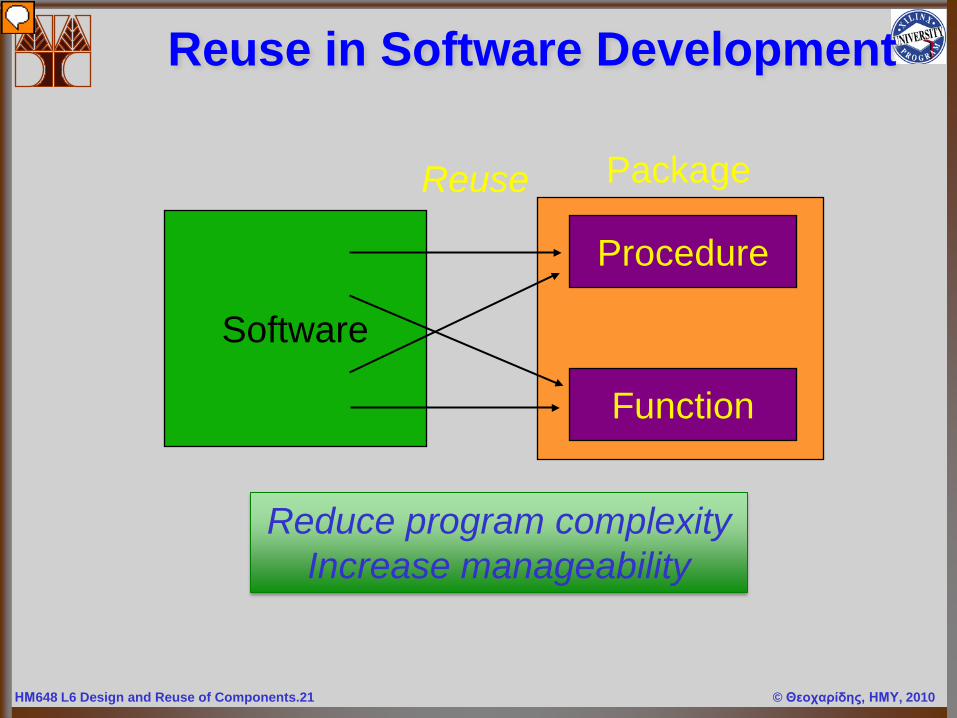
ΗΜ648 L6 Design and Reuse of Components.21 © Θεοχαρίδης, ΗΜΥ, 2010
Reuse in Software Development
Software
Procedure
Function
Reuse
Reduce program complexityIncrease manageability
Package
Presenter
Presentation Notes
During software development, if there a piece of common code that can be shared by a group of software designers, then they don’t have to duplicate their effort to write their own code instead we can write this piece of code as a procedure or function. By grouping a set of close-related procedures and functions, we can form a package that can be used by many designers to develop their system. By doing so, we can reduce the program complexity and increase the manageability.
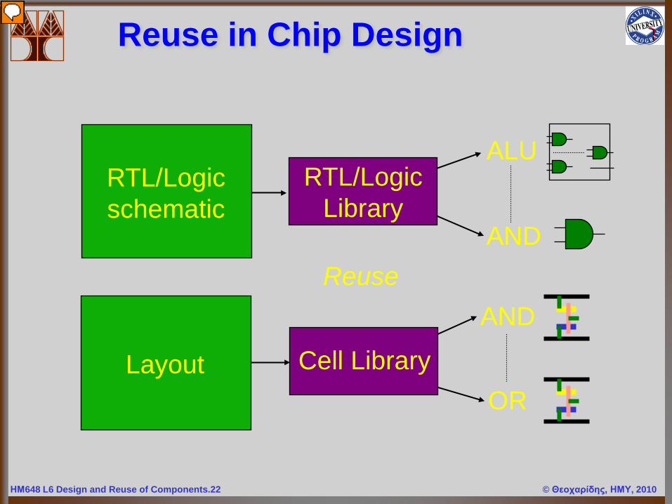
ΗΜ648 L6 Design and Reuse of Components.22 © Θεοχαρίδης, ΗΜΥ, 2010
Reuse in Chip Design
RTL/LogicLibrary
Cell Library
AND
ORLayout
RTL/Logicschematic
ALU
ANDReuse
Presenter
Presentation Notes
The reuse practice has been applied to chip design: 1. In the layout level, designers can reuse the cell library supplied by the vendors. They don’t have to assemble the polygons to form their cells. 2. In the RTL/logic level, designers can reuse pre-designed functional/RTL components. They don’t have to design their RTL components from logic gates and transistors.
ΗΜ648 L6 Design and Reuse of Components.23 © Θεοχαρίδης, ΗΜΥ, 2010
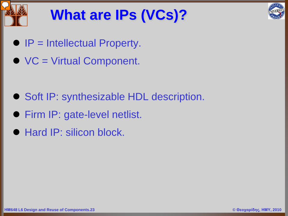
What are IPs (VCs)?
IP = Intellectual Property.
VC = Virtual Component.
Soft IP: synthesizable HDL description.
Firm IP: gate-level netlist.
Hard IP: silicon block.
Presenter
Presentation Notes
In this slide, we try to clarify the terminology of IP and VC. IP is a piece of design (a property) owned by a specific party. VC is a virtual component for your design that will be replaced by a real component. This component is provided by the component owner. We will use IP, VC, and Core interchangeablelly. Soft, firm and hard IPs represent their physical structure. Soft means synthesizable HDL codes. Firm means gate-level netlist. Hard means silicon blocks. Any IPs can be simple designs or very complex designs. For example, an HDL code of an ALU is a soft IP, same as an HDL code of a 68000 processor. Similarly, an AND-gate silicon layout is a hard IP, same as a PCI silicon block.
ΗΜ648 L6 Design and Reuse of Components.24 © Θεοχαρίδης, ΗΜΥ, 2010
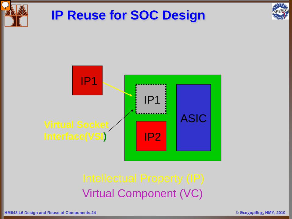
IP Reuse for SOC Design
IP1
IP2ASIC
IP1
Intellectual Property (IP)Virtual Component (VC)
Virtual SocketInterface(VSI)
Presenter
Presentation Notes
One approach to carry out IP-reuse for system LSI (SOC) design is using the virtual component concept. VSI is an interface standard. If an IP is following the VSI standard, the system designer can plug this IP into their design and reuse it as a virtual component.
ΗΜ648 L6 Design and Reuse of Components.25 © Θεοχαρίδης, ΗΜΥ, 2010
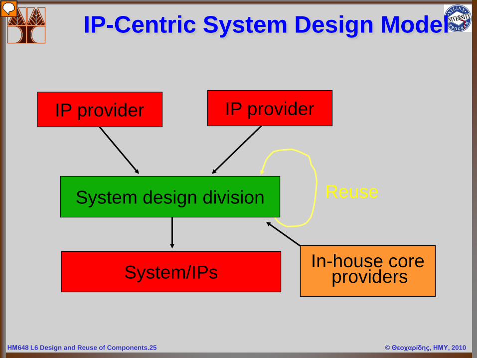
IP-Centric System Design Model
System design division
System/IPs In-house coreproviders
Reuse
IP provider IP provider
Presenter
Presentation Notes
In the IP-centric system design model, the main objective for system designers is to maximally reuse existing IPs and cores for their system design. There are two main sources to obtain IPs and cores. The first one is obtaining IPs/cores from external sources, e.g., IP vendors. The second one is obtaining legacy IPs/cores from internal departments. If possible, after the completion of the system design the system designers can also convert the newly developed design into an IP for later internal reuse or sell to the outside party.
ΗΜ648 L6 Design and Reuse of Components.26 © Θεοχαρίδης, ΗΜΥ, 2010
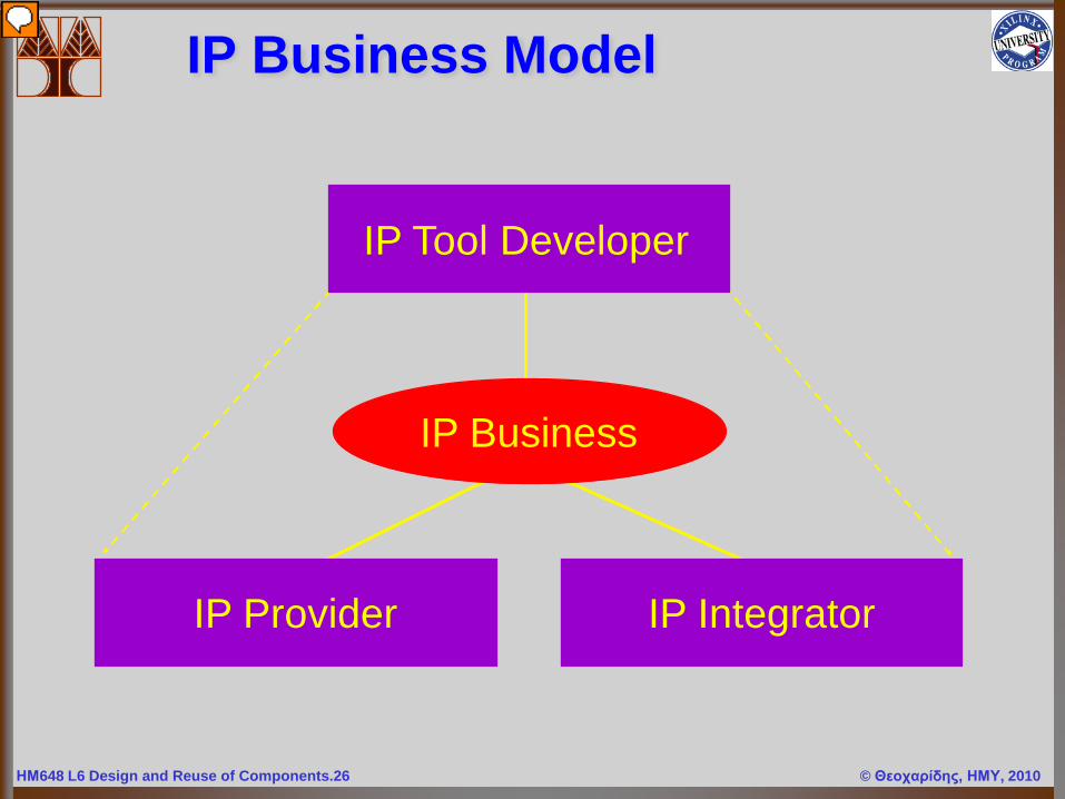
IP Business Model
IP Tool Developer
IP Provider
IP Business
IP Integrator
Presenter
Presentation Notes
A successful IP business depends on three major players: 1. IP provider - supply IPs/cores, 2. IP integrator - IP/core user, system designers, 3. IP tool developer - provide IP-centric design methodology and tool suite, IP/core-reuse methodology and tool suite.
ΗΜ648 L6 Design and Reuse of Components.27 © Θεοχαρίδης, ΗΜΥ, 2010
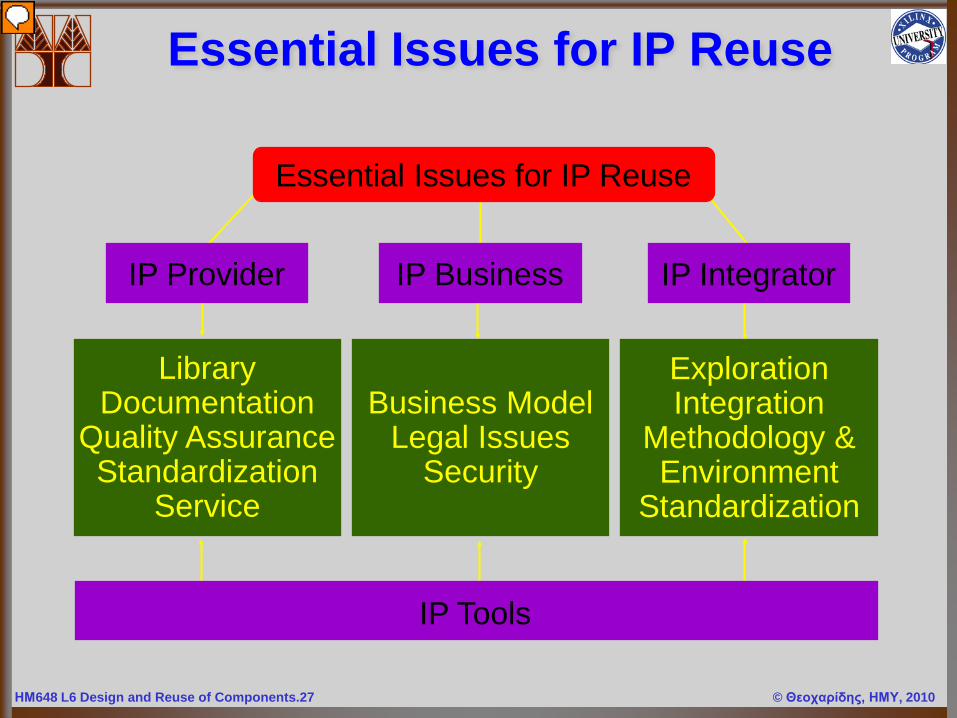
Essential Issues for IP Reuse
Essential Issues for IP Reuse
IP Provider IP Business IP Integrator
LibraryDocumentation
Quality AssuranceStandardization
Service
Business ModelLegal Issues
Security
ExplorationIntegration
Methodology &Environment
Standardization
IP Tools
Presenter
Presentation Notes
This slide shows the essential issues for IP reuse that are divided into four parts: 1. IP provider, 2. IP integrator, 3. IP business, and 4. IP tool developer.
ΗΜ648 L6 Design and Reuse of Components.28 © Θεοχαρίδης, ΗΜΥ, 2010
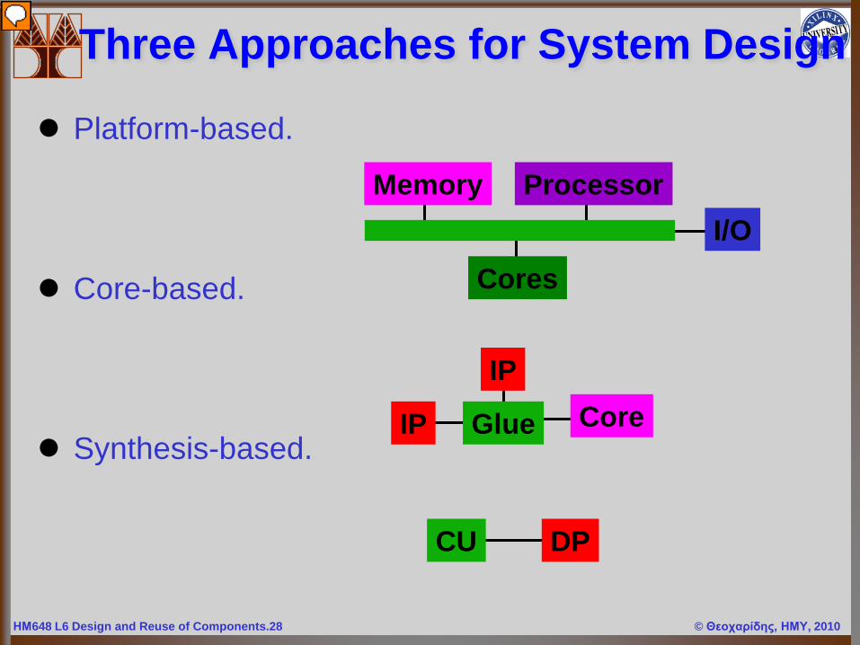
Three Approaches for System Design
Platform-based.
Core-based.
Synthesis-based.
CU DP
ProcessorMemoryI/O
Cores
IP
IPCoreGlue
Presenter
Presentation Notes
There are three approaches for system LSI (SOC) design: 1. Platform: pre-defined design platform/architecture targeted to a specific application (e.g., DSP). 2. Reuse: system integration by reusing IPs/cores. 3. Synthesis: using the traditional RTL synthesis method.
ΗΜ648 L6 Design and Reuse of Components.29 © Θεοχαρίδης, ΗΜΥ, 2010
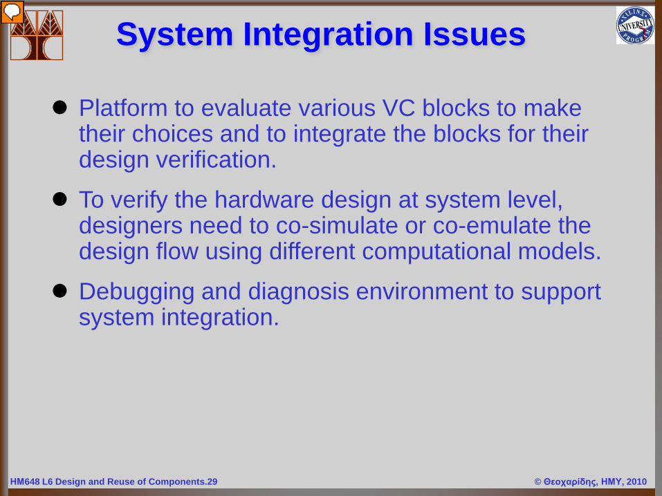
System Integration Issues
Platform to evaluate various VC blocks to make their choices and to integrate the blocks for their design verification.
To verify the hardware design at system level, designers need to co-simulate or co-emulate the design flow using different computational models.
Debugging and diagnosis environment to support system integration.
Presenter
Presentation Notes
This slide and the following two slides addresses the design issues for system integration using the reuse-based design approach.
ΗΜ648 L6 Design and Reuse of Components.30 © Θεοχαρίδης, ΗΜΥ, 2010
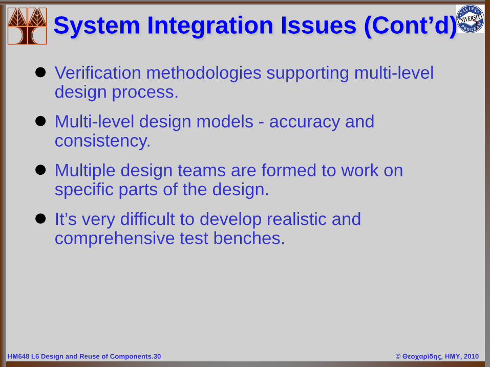
System Integration Issues (Cont’d)
Verification methodologies supporting multi-level design process.
Multi-level design models - accuracy and consistency.
Multiple design teams are formed to work on specific parts of the design.
It’s very difficult to develop realistic and comprehensive test benches.
ΗΜ648 L6 Design and Reuse of Components.31 © Θεοχαρίδης, ΗΜΥ, 2010
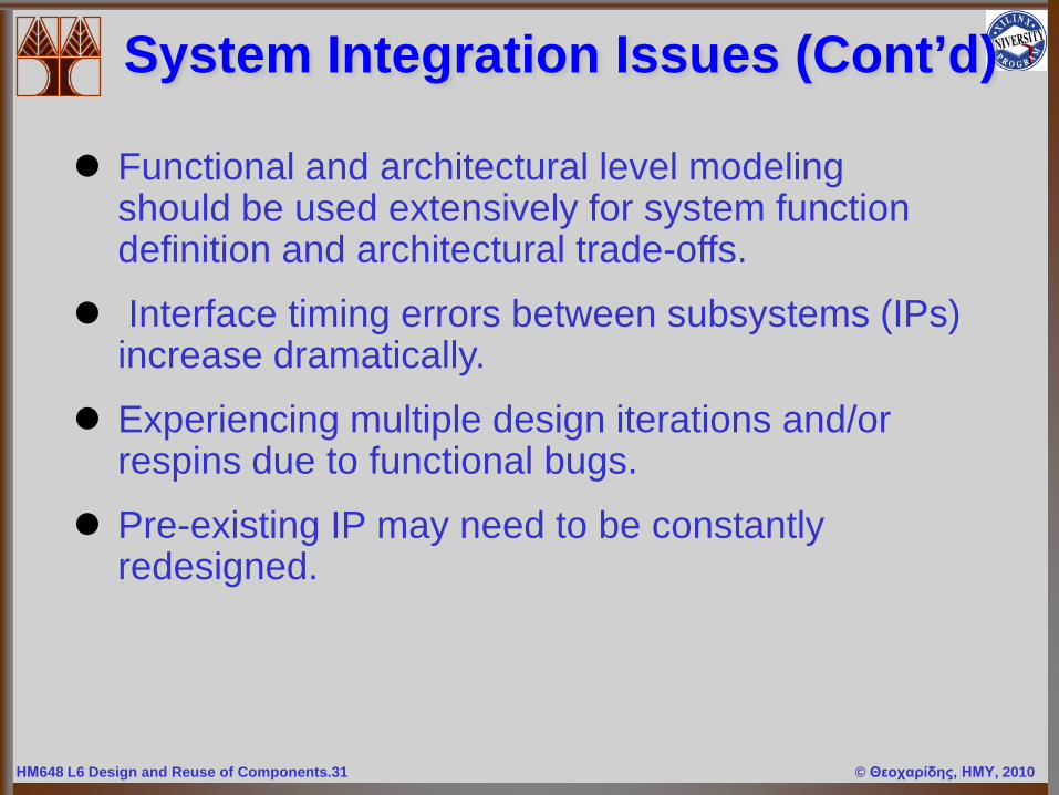
System Integration Issues (Cont’d)
Functional and architectural level modeling should be used extensively for system function definition and architectural trade-offs.
Interface timing errors between subsystems (IPs) increase dramatically.
Experiencing multiple design iterations and/or respins due to functional bugs.
Pre-existing IP may need to be constantly redesigned.
ΗΜ648 L6 Design and Reuse of Components.32 © Θεοχαρίδης, ΗΜΥ, 2010
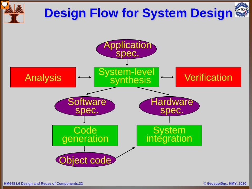
Design Flow for System Design
Applicationspec.
Analysis System-levelsynthesis
Softwarespec.
Codegeneration
Object code
Hardwarespec.
Systemintegration
Verification
Presenter
Presentation Notes
This slide shows a typical system design flow and tasks.
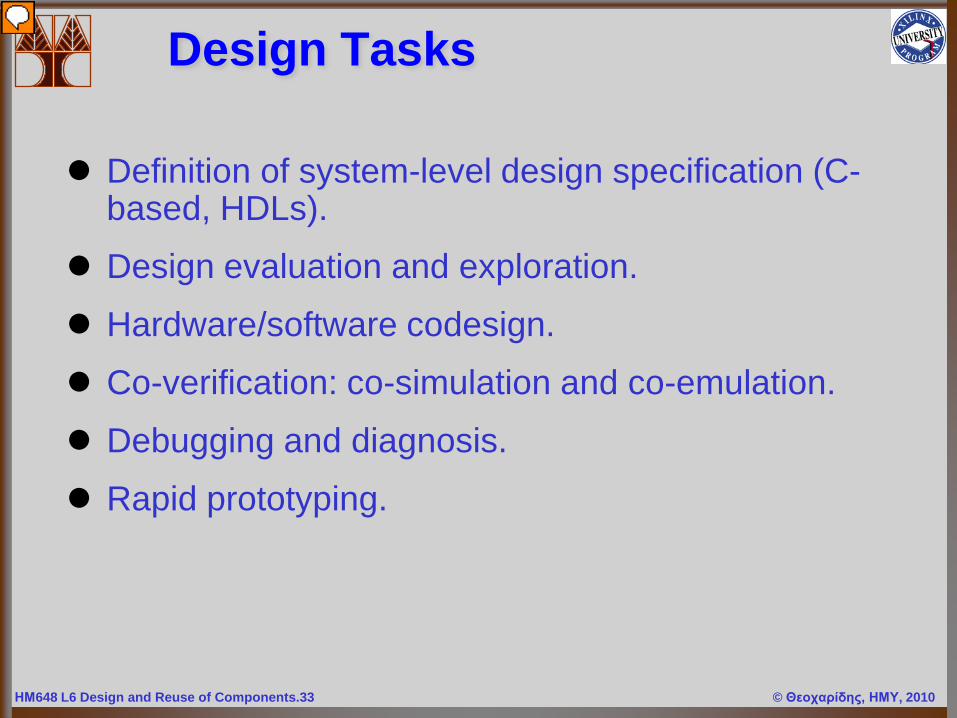
ΗΜ648 L6 Design and Reuse of Components.33 © Θεοχαρίδης, ΗΜΥ, 2010
Design Tasks
Definition of system-level design specification (C-based, HDLs).
Design evaluation and exploration.
Hardware/software codesign.
Co-verification: co-simulation and co-emulation.
Debugging and diagnosis.
Rapid prototyping.
Presenter
Presentation Notes
This slide lists the basic design tasks for system designs.
ΗΜ648 L6 Design and Reuse of Components.34 © Θεοχαρίδης, ΗΜΥ, 2010
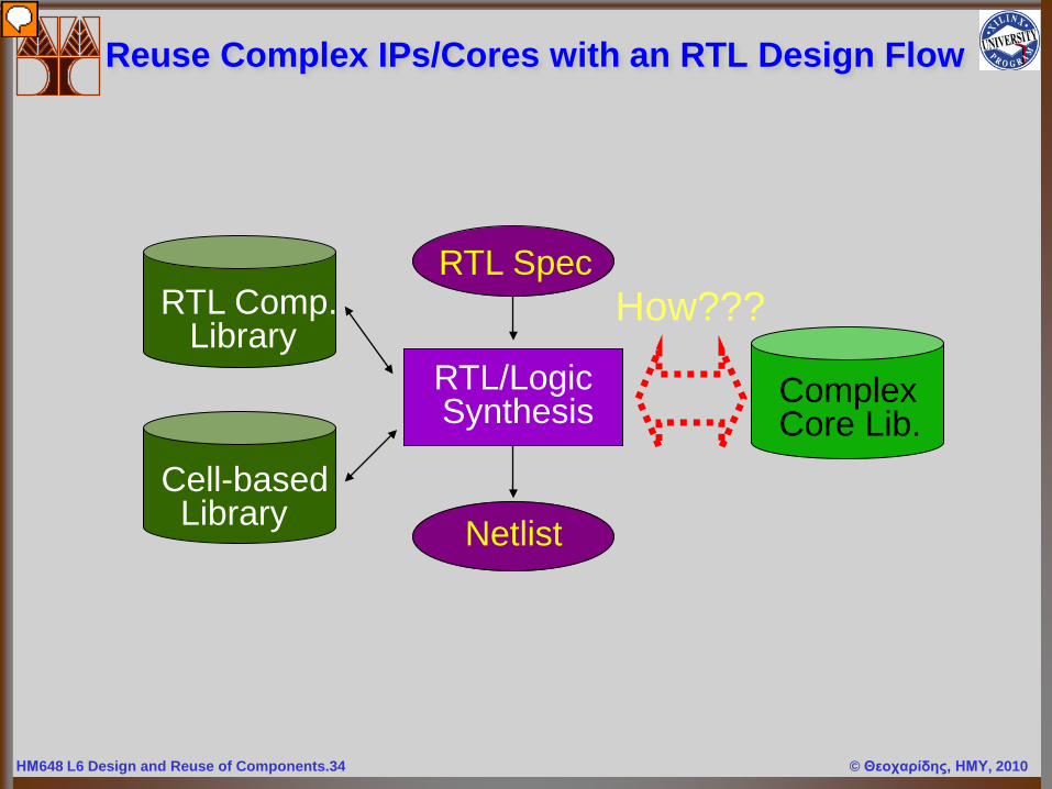
Reuse Complex IPs/Cores with an RTL Design Flow
RTL Spec
RTL/LogicSynthesis
Netlist
RTL Comp.Library
Cell-basedLibrary
ComplexCore Lib.
How???
Presenter
Presentation Notes
How can we use today’s RTL design flow to reuse complex IPs/cores?
ΗΜ648 L6 Design and Reuse of Components.35 © Θεοχαρίδης, ΗΜΥ, 2010
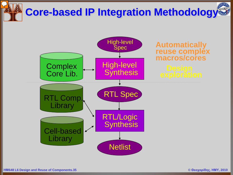
Core-based IP Integration Methodology
High-levelSpec
RTL/LogicSynthesis
Netlist
RTL Comp.Library
Cell-basedLibrary
ComplexCore Lib.
High-levelSynthesis
Automaticallyreuse complexmacros/cores
Designexploration
RTL Spec
Presenter
Presentation Notes
In our approach, we move the design abstraction one level higher than RTL so that we can automatically reuse complex IPs/cores. In addition, we also allow design exploration at higher design level to exploit different design alternatives and reused a variety of IPs/cores.
ΗΜ648 L6 Design and Reuse of Components.36 © Θεοχαρίδης, ΗΜΥ, 2010
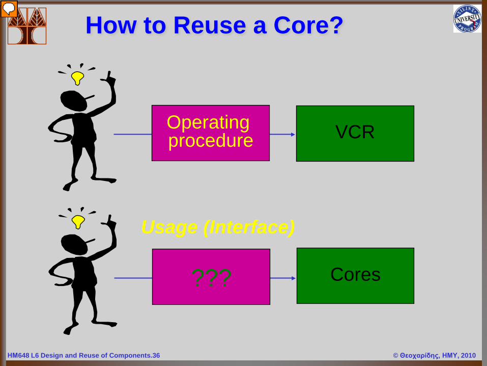
How to Reuse a Core?
VCROperating procedure
Cores???
Usage (Interface)
Presenter
Presentation Notes
Let’s first explain how to reuse a complex core. We use the VCR as an example. As we all know, it’s not an easy job to learn how to set a VCR. We may have to spend hours and carefully go through the manual to just learn the basic setting. Because it’s difficulty, most users simply give up to learn how to set a VCR. The VCR manufactories realize the problem so that they try to develop some easy-to-operate method for the frustrated users. One way is the on-screen setting method. The user can simply follow the on-screen step-by-step instructions to perform basic VCR settings. Once they familiar with the basic setting, they may can become an expert user to customize their setting. We can apply the same approach to teach users how to reuse a complex core. A complex core may contain many features, and there are many different ways to use it for different applications. We may have to provide the user with detail instruction so that the user can easily reuse the core for their design. We call this detail instruction “usage”.
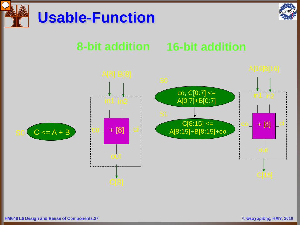
ΗΜ648 L6 Design and Reuse of Components.37 © Θεοχαρίδης, ΗΜΥ, 2010
Usable-Function
C <= A + BS0 + [8]
in1 in2
out
cico
A[8] B[8]
C[8]
+ [8]
in1 in2
out
cico
A[16]B[16]
C[16]
co, C[0:7] <= A[0:7]+B[0:7]
C[8:15] <= A[8:15]+B[8:15]+co
S0
S1
8-bit addition 16-bit addition
Presenter
Presentation Notes
Using an 8-bit adder as a core example, we can easily reuse this core to perform a 8-bit addition computation using one control state. Now, consider how to reuse this core to perform a 16-bit addition computation. We can not simply perform addition in one state instead we have to first perform addition computation of the least significant 8-bit and then the most significant 8-bit. Hence, we need two control states to perform the 16-bit addition when we use the 8-bit adder core.
ΗΜ648 L6 Design and Reuse of Components.38 © Θεοχαρίδης, ΗΜΥ, 2010
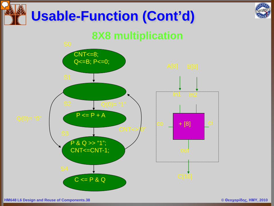
Usable-Function (Cont’d)
+ [8]
in1 in2
out
cico
A[8] B[8]
C[16]
CNT<=8;Q<=B; P<=0;
Q(0)= “1”
Q(0)= “0” P <= P + A
P & Q >> “1”;CNT<=CNT-1;
C <= P & Q
CNT<>”0”
S0
S1
S2
S3
S4
8X8 multiplication
Presenter
Presentation Notes
Similarly, we can devise a control sequence (FSM) to control the core to perform a complex computation such as 8-bit multiplication computation.
ΗΜ648 L6 Design and Reuse of Components.39 © Θεοχαρίδης, ΗΜΥ, 2010
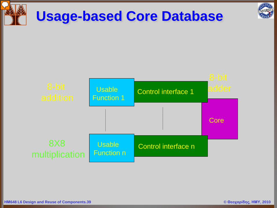
Usage-based Core Database
Core
Control interface 1
Control interface n
UsableFunction 1
UsableFunction n
8-bit adder8-bit
addition
8X8 multiplication
Presenter
Presentation Notes
Based on the usage concept, we can develop a usage-based core database. In the database, each control interface along with a core corresponds to a usable function.
ΗΜ648 L6 Design and Reuse of Components.40 © Θεοχαρίδης, ΗΜΥ, 2010
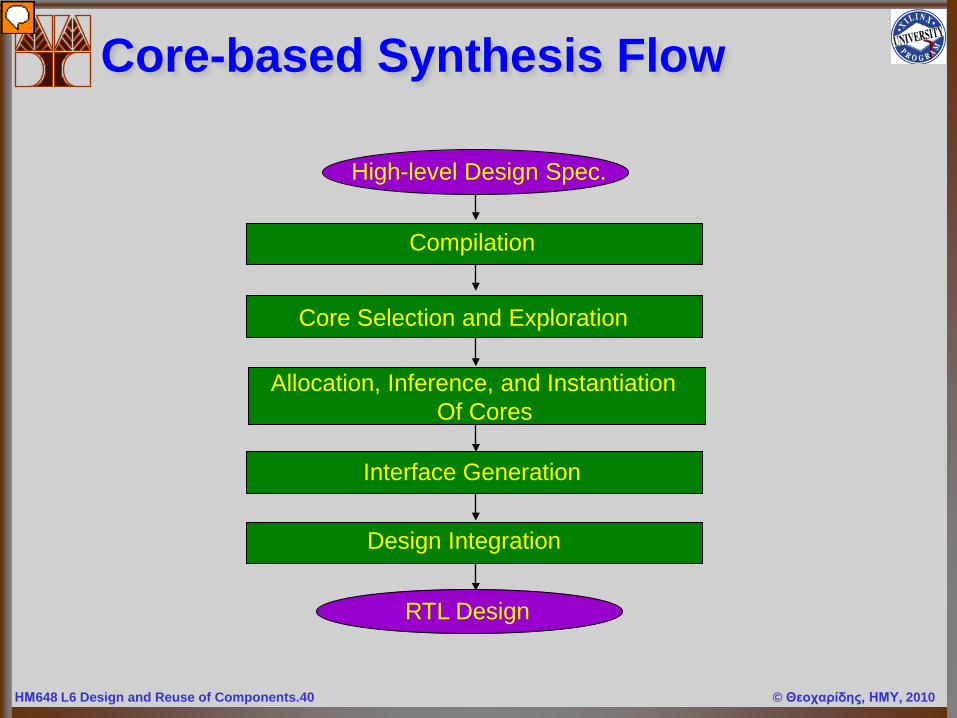
Core-based Synthesis Flow
High-level Design Spec.
Compilation
Core Selection and Exploration
Allocation, Inference, and InstantiationOf Cores
Interface Generation
Design Integration
RTL Design
Presenter
Presentation Notes
This slide shows the proposed reuse automation synthesis flow for complex core reused and design exploration.
ΗΜ648 L6 Design and Reuse of Components.41 © Θεοχαρίδης, ΗΜΥ, 2010
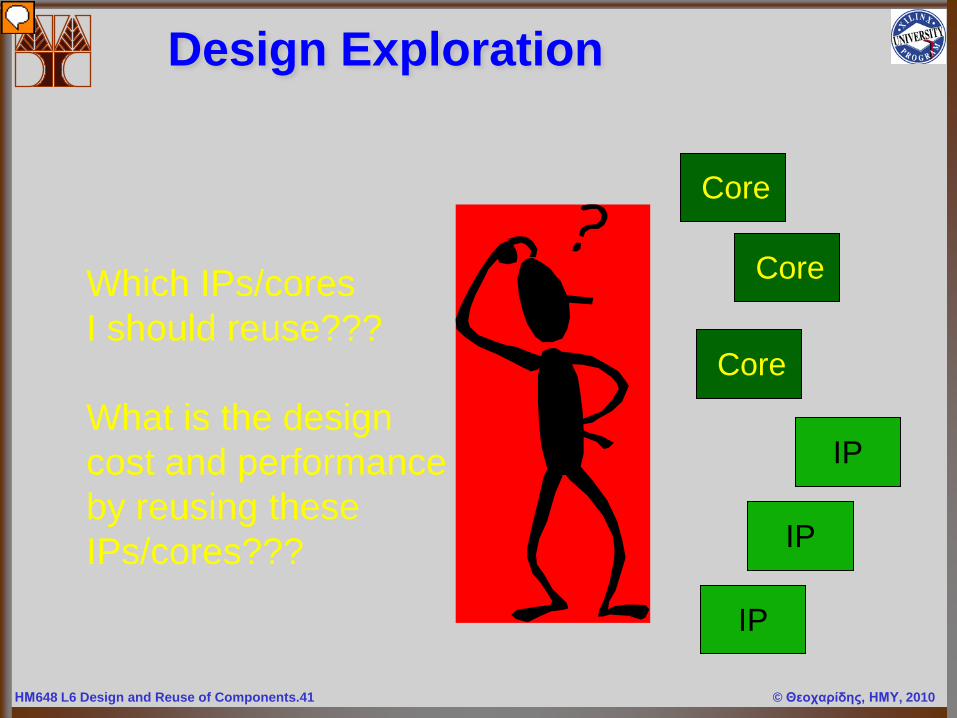
Design Exploration
Core
IP
IP
IP
Core
Core
Which IPs/coresI should reuse???
What is the designcost and performanceby reusing theseIPs/cores???
Presenter
Presentation Notes
There are too many IPs/cores market, we need a design exploration method to assist our design decision on IP/core selection.
ΗΜ648 L6 Design and Reuse of Components.42 © Θεοχαρίδης, ΗΜΥ, 2010
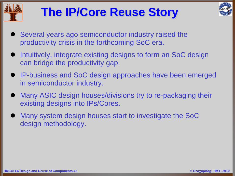
The IP/Core Reuse Story
Several years ago semiconductor industry raised the productivity crisis in the forthcoming SoC era.
Intuitively, integrate existing designs to form an SoC design can bridge the productivity gap.
IP-business and SoC design approaches have been emerged in semiconductor industry.
Many ASIC design houses/divisions try to re-packaging their existing designs into IPs/Cores.
Many system design houses start to investigate the SoC design methodology.
ΗΜ648 L6 Design and Reuse of Components.43 © Θεοχαρίδης, ΗΜΥ, 2010
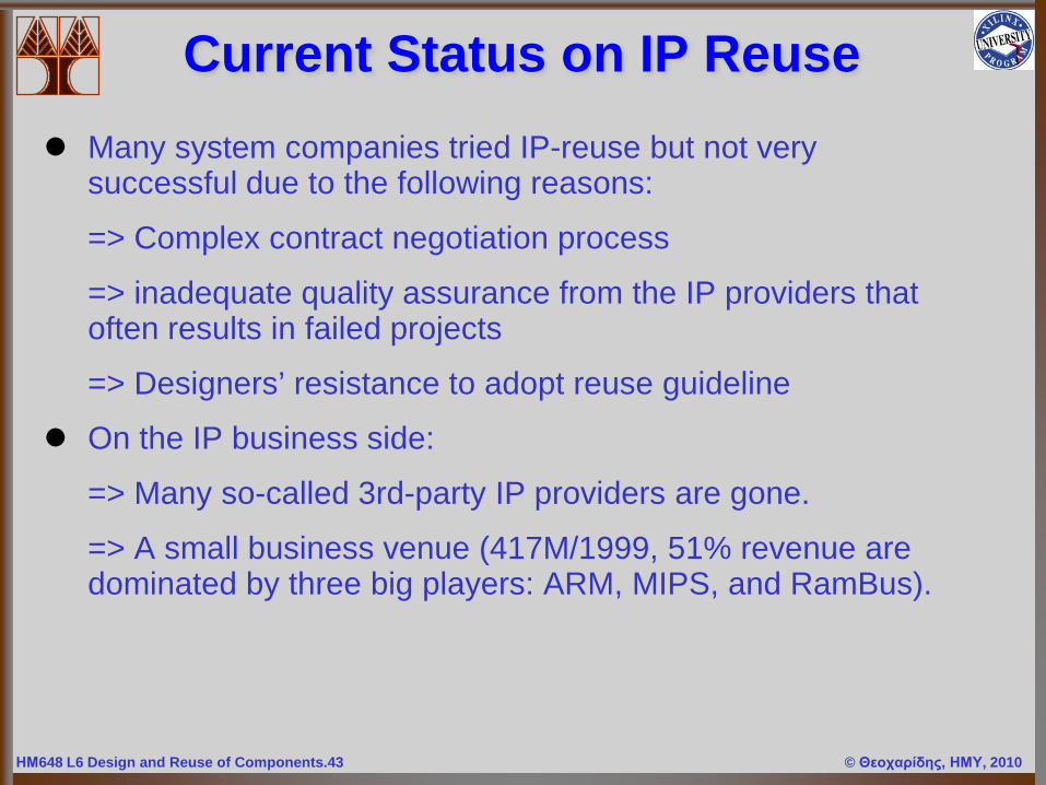
Current Status on IP Reuse Many system companies tried IP-reuse but not very
successful due to the following reasons:
=> Complex contract negotiation process
=> inadequate quality assurance from the IP providers that often results in failed projects
=> Designers’ resistance to adopt reuse guideline
On the IP business side:
=> Many so-called 3rd-party IP providers are gone.
=> A small business venue (417M/1999, 51% revenue are dominated by three big players: ARM, MIPS, and RamBus).
ΗΜ648 L6 Design and Reuse of Components.44 © Θεοχαρίδης, ΗΜΥ, 2010
Designers’ Perspective on Reuse
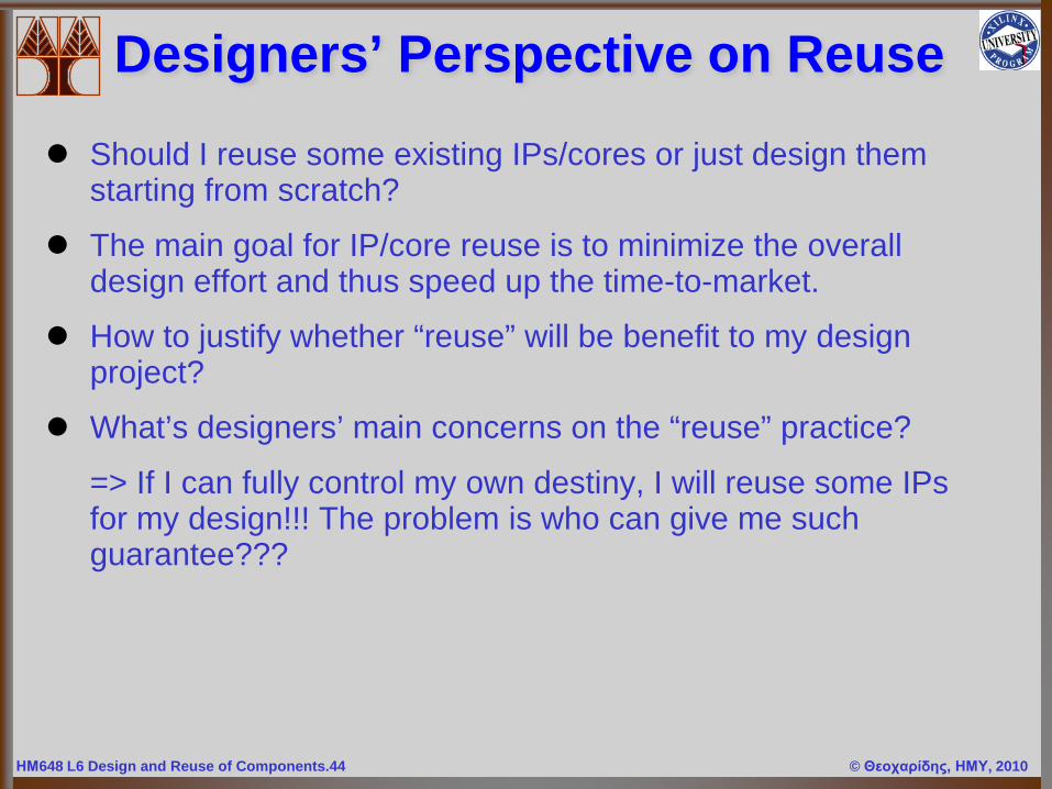
Should I reuse some existing IPs/cores or just design them starting from scratch?
The main goal for IP/core reuse is to minimize the overall design effort and thus speed up the time-to-market.
How to justify whether “reuse” will be benefit to my design project?
What’s designers’ main concerns on the “reuse” practice?
=> If I can fully control my own destiny, I will reuse some IPs for my design!!! The problem is who can give me such guarantee???
ΗΜ648 L6 Design and Reuse of Components.45 © Θεοχαρίδης, ΗΜΥ, 2010
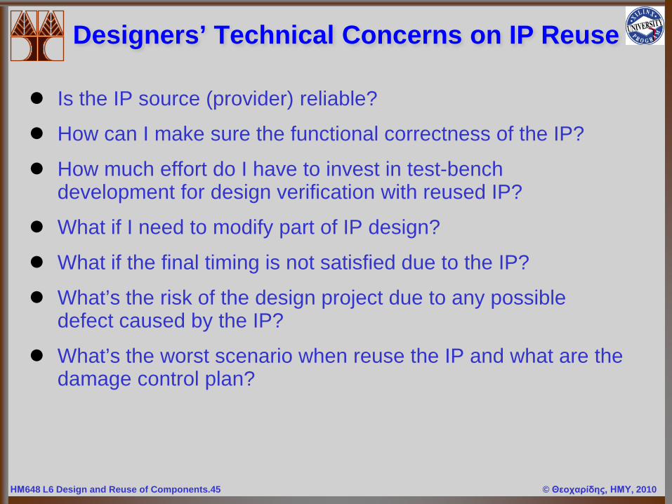
Designers’ Technical Concerns on IP Reuse
Is the IP source (provider) reliable?
How can I make sure the functional correctness of the IP?
How much effort do I have to invest in test-bench development for design verification with reused IP?
What if I need to modify part of IP design?
What if the final timing is not satisfied due to the IP?
What’s the risk of the design project due to any possible defect caused by the IP?
What’s the worst scenario when reuse the IP and what are the damage control plan?
ΗΜ648 L6 Design and Reuse of Components.46 © Θεοχαρίδης, ΗΜΥ, 2010
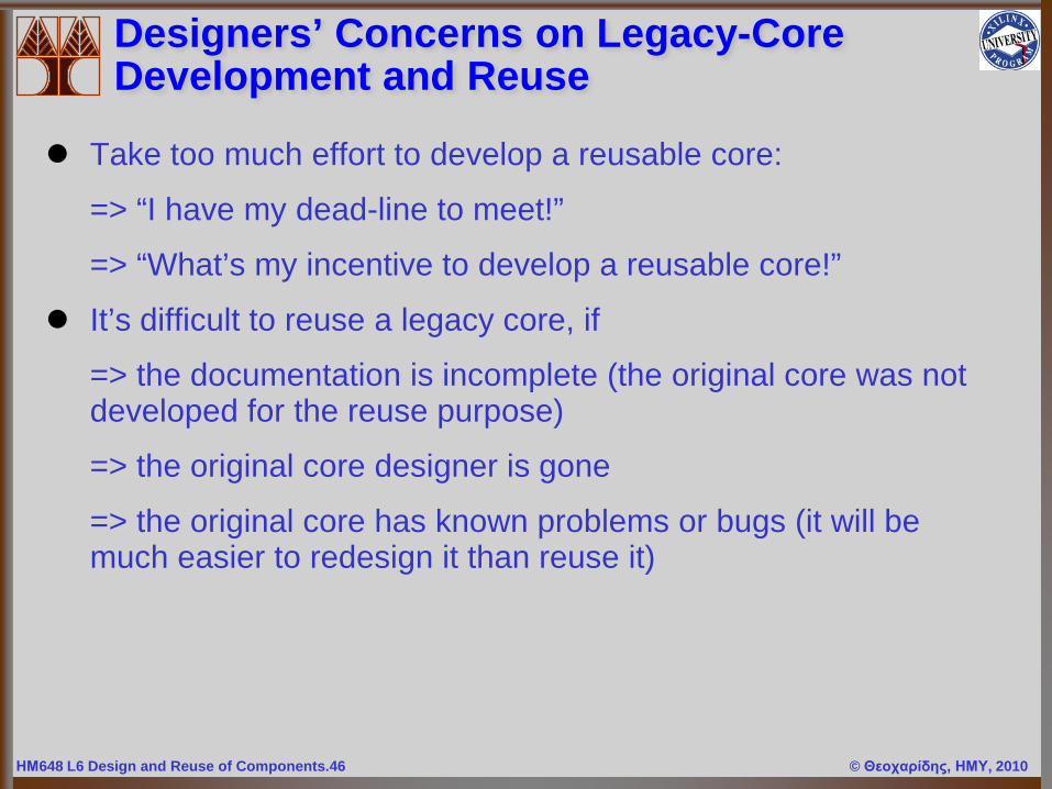
Designers’ Concerns on Legacy-Core Development and Reuse
Take too much effort to develop a reusable core:
=> “I have my dead-line to meet!”
=> “What’s my incentive to develop a reusable core!”
It’s difficult to reuse a legacy core, if
=> the documentation is incomplete (the original core was not developed for the reuse purpose)
=> the original core designer is gone
=> the original core has known problems or bugs (it will be much easier to redesign it than reuse it)
ΗΜ648 L6 Design and Reuse of Components.47 © Θεοχαρίδης, ΗΜΥ, 2010
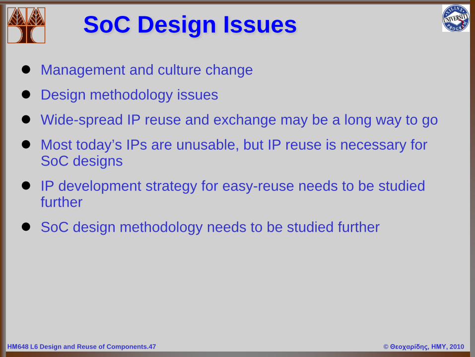
SoC Design Issues
Management and culture change
Design methodology issues
Wide-spread IP reuse and exchange may be a long way to go
Most today’s IPs are unusable, but IP reuse is necessary for SoC designs
IP development strategy for easy-reuse needs to be studied further
SoC design methodology needs to be studied further
ΗΜ648 L6 Design and Reuse of Components.48 © Θεοχαρίδης, ΗΜΥ, 2010
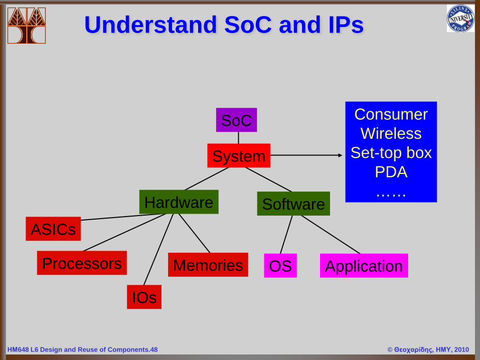
Understand SoC and IPs
SoC
System
Hardware Software
OS ApplicationProcessors Memories
IOs
ConsumerWireless
Set-top boxPDA……
ASICs
ΗΜ648 L6 Design and Reuse of Components.49 © Θεοχαρίδης, ΗΜΥ, 2010
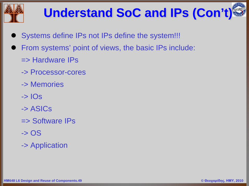
Understand SoC and IPs (Con’t) Systems define IPs not IPs define the system!!! From systems’ point of views, the basic IPs include:
=> Hardware IPs-> Processor-cores-> Memories-> IOs-> ASICs=> Software IPs-> OS-> Application
ΗΜ648 L6 Design and Reuse of Components.50 © Θεοχαρίδης, ΗΜΥ, 2010
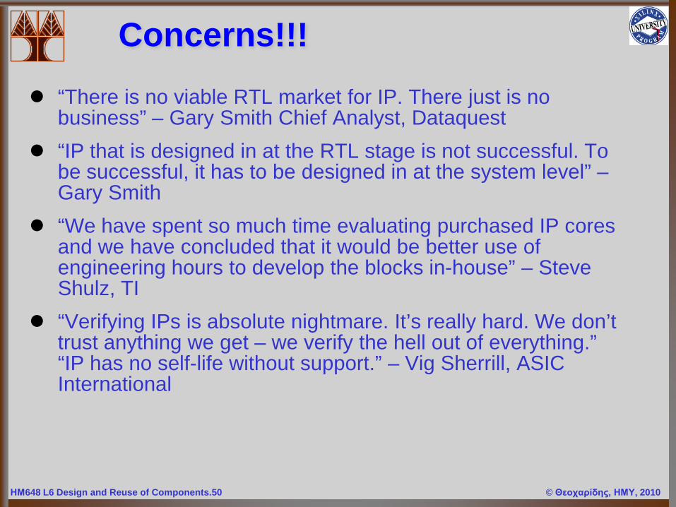
Concerns!!! “There is no viable RTL market for IP. There just is no
business” – Gary Smith Chief Analyst, Dataquest “IP that is designed in at the RTL stage is not successful. To
be successful, it has to be designed in at the system level” –Gary Smith
“We have spent so much time evaluating purchased IP cores and we have concluded that it would be better use of engineering hours to develop the blocks in-house” – Steve Shulz, TI
“Verifying IPs is absolute nightmare. It’s really hard. We don’t trust anything we get – we verify the hell out of everything.” “IP has no self-life without support.” – Vig Sherrill, ASIC International
ΗΜ648 L6 Design and Reuse of Components.51 © Θεοχαρίδης, ΗΜΥ, 2010
SoC and IPs (Con’t)
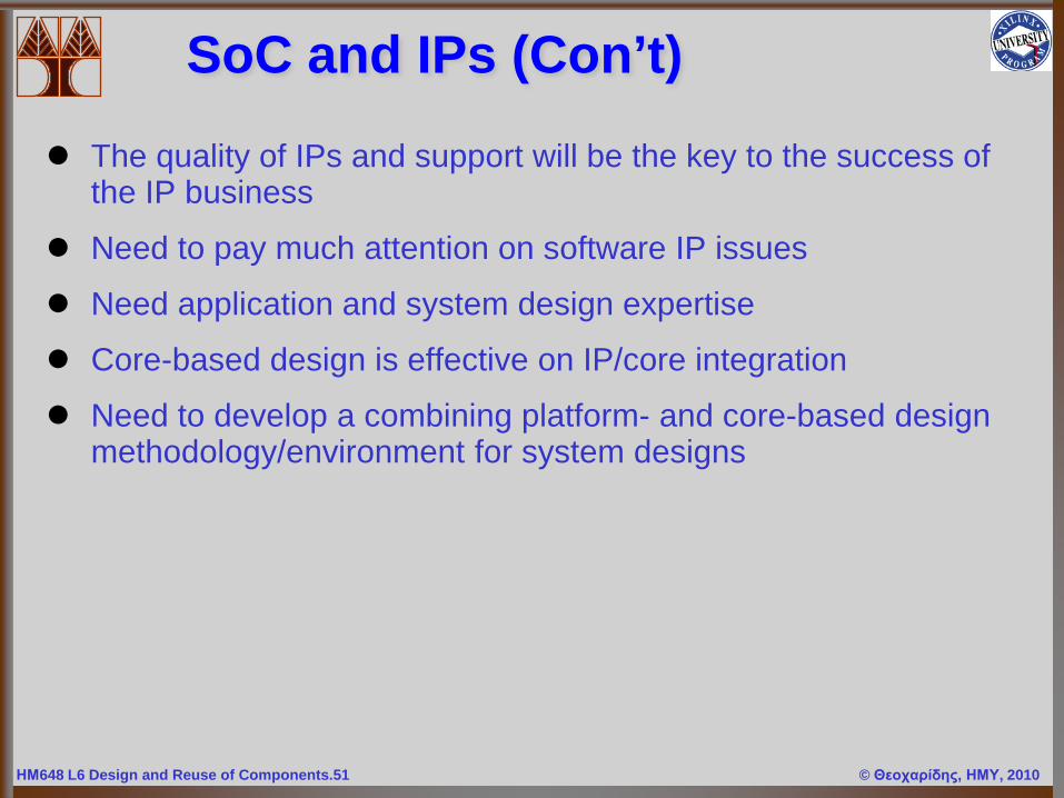
The quality of IPs and support will be the key to the success of the IP business
Need to pay much attention on software IP issues
Need application and system design expertise
Core-based design is effective on IP/core integration
Need to develop a combining platform- and core-based design methodology/environment for system designs
ΗΜ648 L6 Design and Reuse of Components.52 © Θεοχαρίδης, ΗΜΥ, 2010
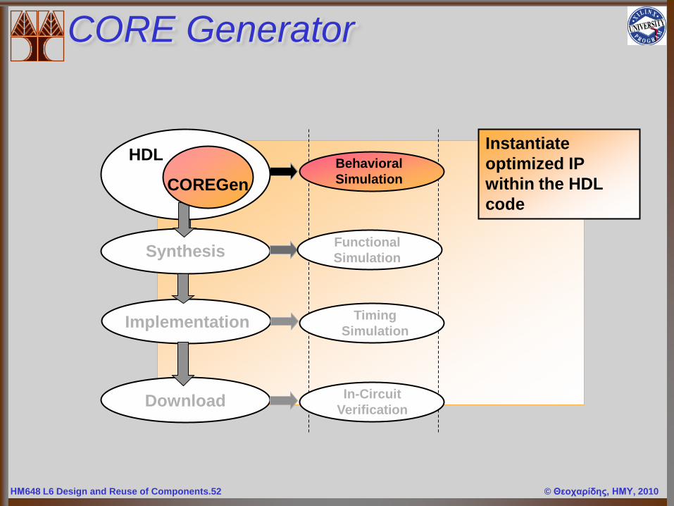
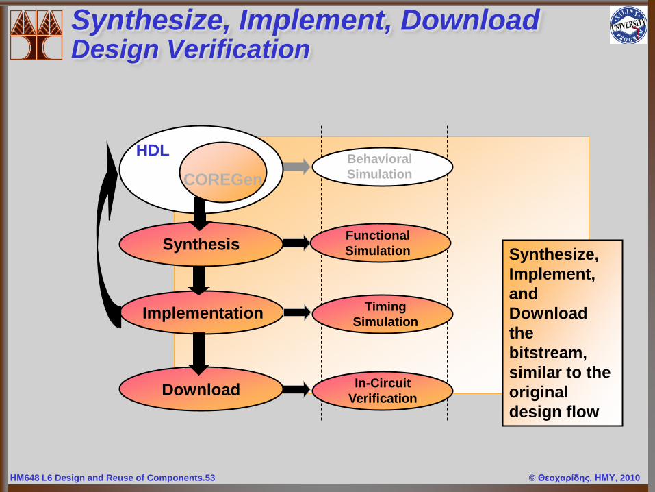
BehavioralSimulation
CORE Generator
Synthesis
Implementation
Download
Functional Simulation
TimingSimulation
In-Circuit Verification
HDL
COREGen
Instantiate optimized IP within the HDL code
ΗΜ648 L6 Design and Reuse of Components.53 © Θεοχαρίδης, ΗΜΥ, 2010
BehavioralSimulation
Synthesize, Implement, DownloadDesign Verification
Synthesis
Implementation
Download
Functional Simulation
TimingSimulation
In-Circuit Verification
HDL
COREGen
Synthesize, Implement, and Download the bitstream, similar to the original design flow
ΗΜ648 L6 Design and Reuse of Components.54 © Θεοχαρίδης, ΗΜΥ, 2010
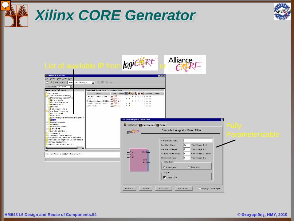
Xilinx CORE Generator
List of available IP from or
FullyParameterizable
Presenter
Presentation Notes
.EDN (EDIF implementation netlist) .XCO (core implementation data file / log file) Optional: .ASY Foundation or Innoveda symbols .VEO Verilog template .VHO VHDL template
ΗΜ648 L6 Design and Reuse of Components.55 © Θεοχαρίδης, ΗΜΥ, 2010
IP CENTERhttp://www.xilinx.com/ipcenter
$P Reed Solomon$3GPP Turbo Code$P Viterbi Decoder$P Convolution Encoder $P Interleaver/De-interleaverP LFSRP 1D DCTP DA FIR P MACP MAC-based FIR filterFixed FFTs 16, 64, 256, 1024 pointsP FFT - 32 PointP Sine CosineP Direct Digital Synthesizer P Cascaded Integrator CombP Bit CorrelatorP Digital Down Converter
P Asynchronous FIFOP Block Memory modulesP Distributed MemoryP Distributed Mem EnhanceP Sync FIFO (SRL16)P Sync FIFO (Block RAM)P CAM (SRL16)
P Binary DecoderP Two's ComplementP Shift Register RAM/FFP Gate modulesP Multiplexer functionsP Registers, FF & latch basedP Adder/SubtractorP AccumulatorP ComparatorP Binary Counter
P Multiplier Generator- Parallel Multiplier - Dyn Constant Coefficient Mult- Serial Sequential Multiplier- Multiplier Enhancements
P DividerP CORDIC
Base Functions$P PCI 64/66$PS PCI 32/33$P PCI-X 64/66
8B/10B Encoder/Decoder$ POS-PHY L3$ POS-PHY L4$ Flexbus 4$ RapidIO PHY Layer$S HDLC 1 and 32 channel$S G.711 PCM Cores$S ADPCM 32 & 64 channel
Memory FunctionsDSP Functions
PCI
Math Functions
Networking
$ - License Fee, P - Parameterized, S - Project License Available,BOLD – Available in the Xilinx Blockset for the System Generator for DSP
Xilinx IP Solutions: Core Gen
Presenter
Presentation Notes
Although continuously increasing, the list of IP is limited and you will not always find the function of interest. Several options are available in that case: build the required function from lower level block IP or choose a mix-mode where part of the function is specified in HDL or schematic and the rest in IP.
ΗΜ648 L6 Design and Reuse of Components.56 © Θεοχαρίδης, ΗΜΥ, 2010
Core Generator: Summary
CORE Generator Advantages
Can quickly access and generate existing functions No need to reinvent the wheel and re-design a block if it meets
specifications IP is optimized for the specified architecture
Disadvantages IP doesn’t always do exactly what you are looking for Need to understand signals and parameters and match them to your
specification Dealing with black box and have little information on how the function
is implemented
ΗΜ648 L6 Design and Reuse of Components.57 © Θεοχαρίδης, ΗΜΥ, 2010
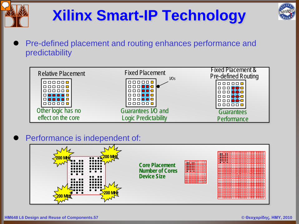
Relative Placement
Other logic has noeffect on the core
Fixed Placement & Pre-defined Routing
GuaranteesPerformance
Guarantees I/O andLogic Predictability
Fixed PlacementI/Os
Xilinx Smart-IP Technology
200 MHz
200 MHz
200 MHz
Core PlacementNumber of CoresDevice Size
200 MHz
Pre-defined placement and routing enhances performance and predictability
Performance is independent of:
Presenter
Presentation Notes
With relative placement of the logic within a core, you get logic predictability. Because the logic has consistent internal placement, the performance of a core remains constant regardless of its position in the device. This is the intelligent software part of Smart-IP technology. In addition to the modular routing capability, we can keep track of the relative location of a core’s logic. Hence, we can floorplan the core or fix its placement with respect to the I/O. For guaranteed performance, we can even fix the placement and predefine the routing. For example, the Xilinx DSP CORES use only relative placement, but for the more performance-sensitive PCI design we use the fixed placement and predefined routing strategy. Designs can be migrated to larger devices without any performance degradation. Because of the use of regular local logic and interconnect as well as segmented routing, the IP modules can be placed anywhere on the device without impacting performance. Because the IP modules use regular local logic and interconnect, you can also place multiple copies of the same module on a device and they will ALL continue to function at the published performance speeds. For the same reasons, you can also migrate an IP module from smaller devices to larger devices without degrading the module’s performance.
ΗΜ648 L6 Design and Reuse of Components.58 © Θεοχαρίδης, ΗΜΥ, 2010
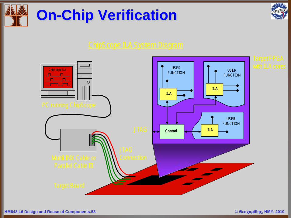
On-Chip Verification
Control
USERFUNCTION
ILA
USERFUNCTION
USERFUNCTION
ILA
ILA
Chipscope ILA
PC running ChipScope
MultiLINX Cable orParallel Cable III
JTAGConnection
Target Board
Target FPGAwith ILA cores
JTAG
ChipScope ILA System Diagram
ΗΜ648 L6 Design and Reuse of Components.59 © Θεοχαρίδης, ΗΜΥ, 2010
CoreGenerator
Use in lab 4 at your own responsibility/risk!
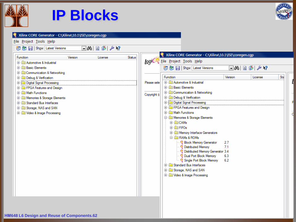
Useful in creating modules such as memory, FIFO queues, custom arithmetic modules, etc.
Start by creating a new project in CoreGenerator, or a new CoreGenerator module in Xilinx ISE.
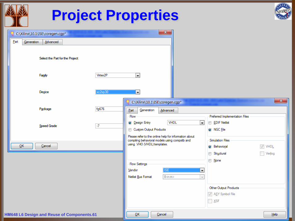
Make sure your FPGA specs are fed into the CoreGenerator project properties!!!
Once you specify the targeted FPGA, then you can browse through the components.
ΗΜ648 L6 Design and Reuse of Components.60 © Θεοχαρίδης, ΗΜΥ, 2010
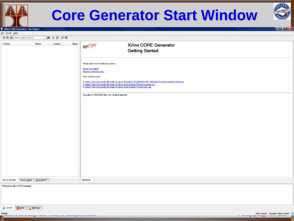
Core Generator Start Window
ΗΜ648 L6 Design and Reuse of Components.61 © Θεοχαρίδης, ΗΜΥ, 2010
Project Properties
ΗΜ648 L6 Design and Reuse of Components.62 © Θεοχαρίδης, ΗΜΥ, 2010
IP Blocks
ΗΜ648 L6 Design and Reuse of Components.63 © Θεοχαρίδης, ΗΜΥ, 2010
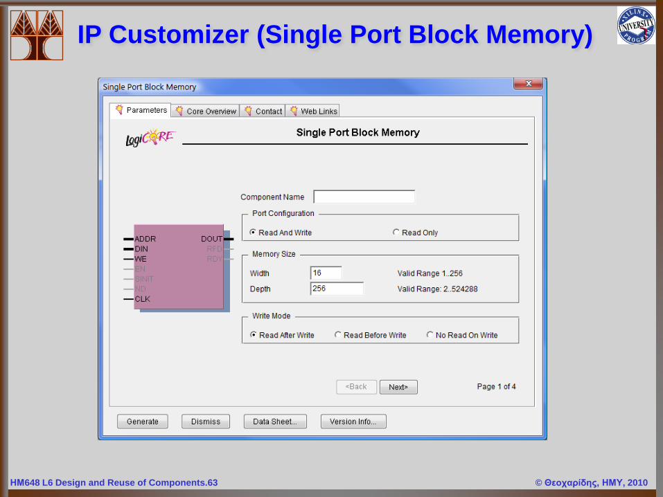
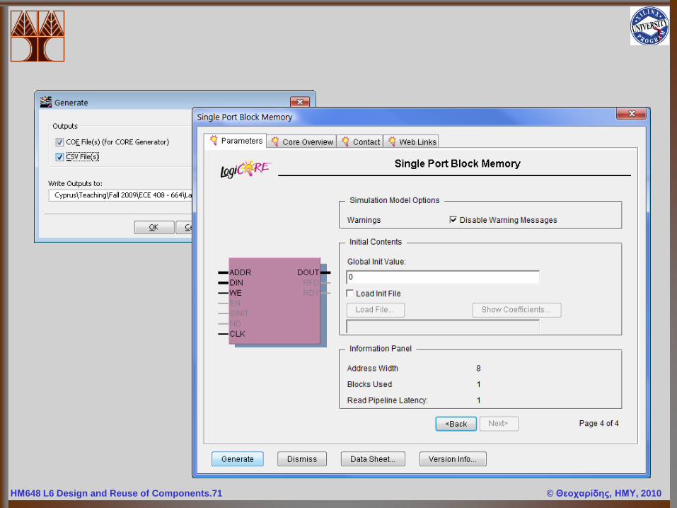
IP Customizer (Single Port Block Memory)
ΗΜ648 L6 Design and Reuse of Components.64 © Θεοχαρίδης, ΗΜΥ, 2010
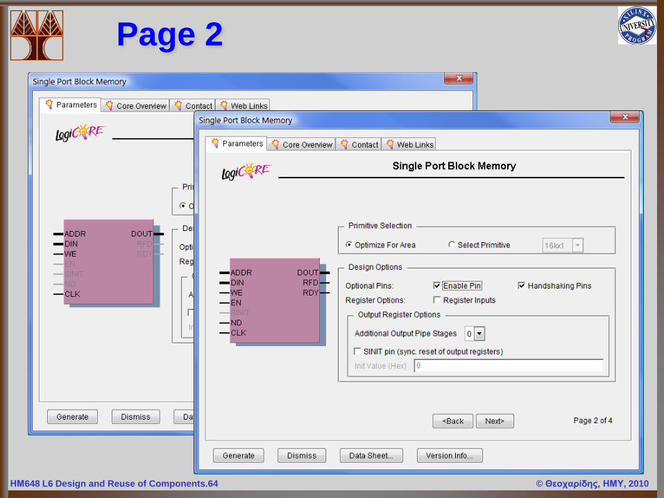
Page 2
ΗΜ648 L6 Design and Reuse of Components.65 © Θεοχαρίδης, ΗΜΥ, 2010
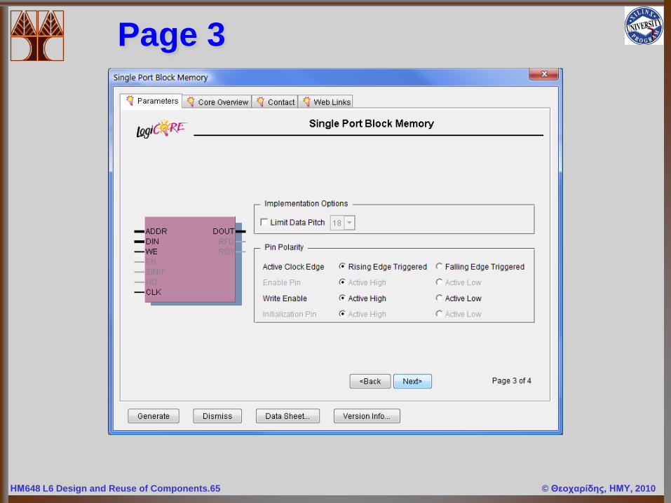
Page 3
ΗΜ648 L6 Design and Reuse of Components.66 © Θεοχαρίδης, ΗΜΥ, 2010
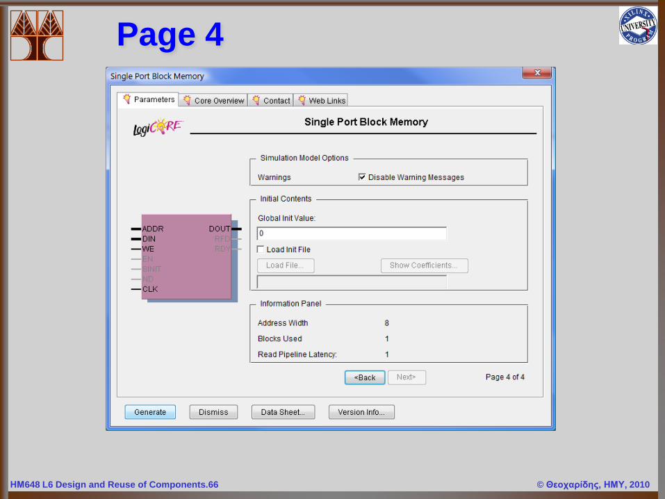
Page 4
ΗΜ648 L6 Design and Reuse of Components.67 © Θεοχαρίδης, ΗΜΥ, 2010
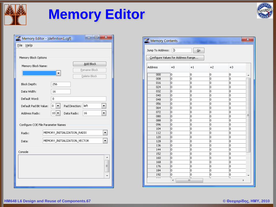
Memory Editor
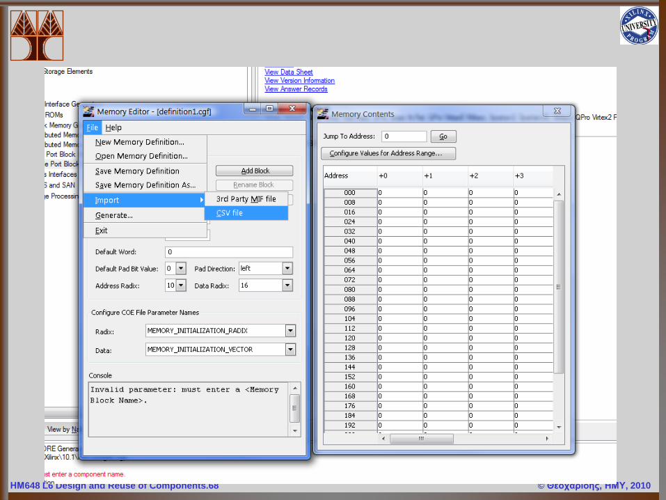
ΗΜ648 L6 Design and Reuse of Components.68 © Θεοχαρίδης, ΗΜΥ, 2010
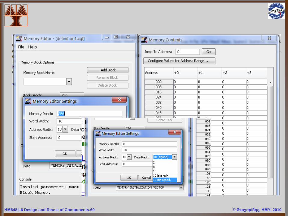
ΗΜ648 L6 Design and Reuse of Components.69 © Θεοχαρίδης, ΗΜΥ, 2010
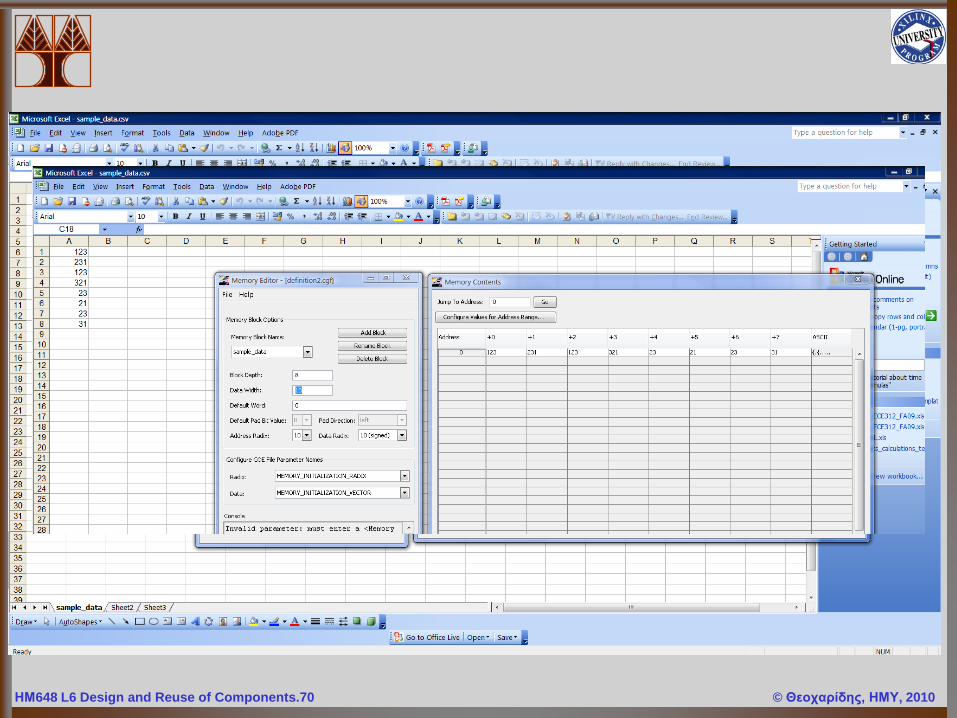
ΗΜ648 L6 Design and Reuse of Components.70 © Θεοχαρίδης, ΗΜΥ, 2010
ΗΜ648 L6 Design and Reuse of Components.71 © Θεοχαρίδης, ΗΜΥ, 2010